Cirrus Logic EP7309 User Manual
Page 13
DS507F2
Copyright Cirrus Logic, Inc. 2011
(All Rights Reserved)
13
EP7309
High-Performance, Low-Power System on Chip
Note:
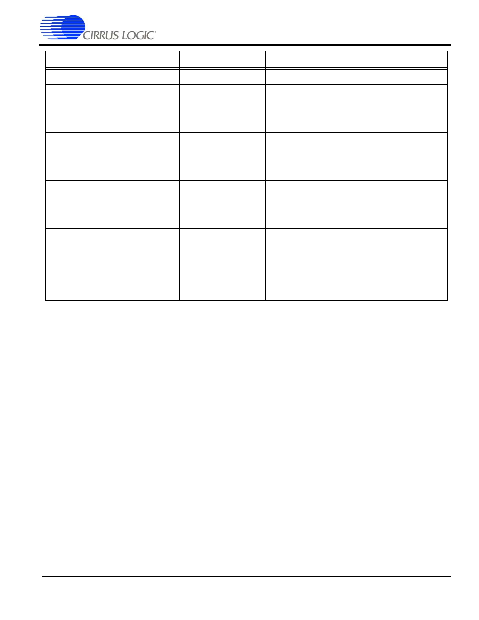
1) Total power consumption = IDD
CORE
x
2.5 V + IDD
IO
x
3.3 V
2) A typical design will provide 3.3 V to the I/O supply (i.e., V
DDIO
), and 2.5 V to the remaining logic. This is to allow the I/O to be
compatible with 3.3 V powered external logic (i.e., 3.3 V SDRAMs).
2) Pull-up current = 50 µA typical at V
DD
= 3.3 V.
CI/O
Transceiver capacitance
8
-
10.0
pF
IDD
STANDBY
@ 25 C
Standby current consumption
1
Core, Osc, RTC @2.5 V
I/O @ 3.3 V
-
-
77
41
-
-
µA
Only nPOR, nPWRFAIL,
nURESET, PE0, PE1, and RTS
are driven, while all other float,
VIH = V
DD
± 0.1 V,
VIL = GND ± 0.1 V
IDD
STANDBY
@ 70 C
Standby current consumption
1
Core, Osc, RTC @2.5 V
I/O @ 3.3 V
-
-
-
-
570
111
µA
Only nPOR, nPWRFAIL,
nURESET, PE0, PE1, and RTS
are driven, while all other float,
VIH = V
DD
± 0.1 V,
VIL = GND ± 0.1 V
IDD
STANDBY
@ 85 C
Standby current consumption
1
Core, Osc, RTC @2.5 V
I/O @ 3.3 V
-
-
-
-
1693
163
µA
Only nPOR, nPWRFAIL,
nURESET, PE0, PE1, and RTS
are driven, while all other float,
VIH = V
DD
± 0.1 V,
VIL = GND ± 0.1 V
IDD
idle
at 74 MHz
Idle current consumption
1
Core, Osc, RTC @2.5 V
I/O @ 3.3 V
-
-
6
10
-
-
mA
Both oscillators running, CPU
static, Cache enabled, LCD
disabled, VIH = V
DD
± 0.1 V, VIL
= GND ± 0.1 V
VDD
STANDBY
Standby supply voltage
2.0
-
-
V
Minimum standby voltage for
state retention, internal SRAM
cache, and RTC operation only
a.
Refer to the strength column in the pin assignment tables for all package types.
b.
Assumes buffer has no pull-up or pull-down resistors.
c.
The leakage value given assumes that the pin is configured as an input pin but is not currently being driven.
Symbol
Parameter
Min
Typ
Max
Unit
Conditions