3 afe scaling range, An366 – Cirrus Logic AN366 User Manual
Page 4
AN366
4
AN366REV2
3.3 AFE Scaling Range
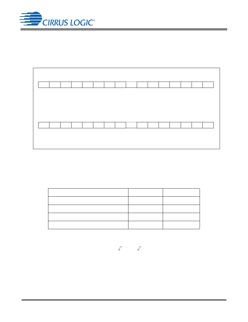
The CS5484 full scale RMS register values are commonly reported as 0.6 when the inputs are at a maximum
level. The ratio of the AFE inputs to full scale defines the reference point for all other input levels. The 24-bit
I1
RMS
and V1
RMS
registers are defined in Figure 2. Note that the digital scaling for RMS current (positive only)
does not match the scaling for power (signed). Section 6.2 Main Calibration Flow Diagram Using the CDB5484
on page 29 describes the scaling ratio of the AFE inputs when maximum input levels are applied.
Use Equation 1 to convert the hexadecimal value to a decimal value:
Using Equation 1, the following key values are identified:
If a sine wave is applied to the voltage channel input at full scale, then the peak voltage can be determined using
Equation 2:
The V
PEAK
register will have a maximum input margin of 15%, which prevents clipping.
The CS5480/84/90 provides a current channel scale register that allows a small load current during calibration.
By default, the range is 0.6 (full-scale current load), but this value can be adjusted according to the load current
available.
Key RMS Register Values Range (0 to 1)
Decimal Value
Register Value
Maximum RMS Register
1
0xFFFFFF
Maximum RMS Input
0.6
0x999999
Half RMS Input
0.36
0x5C28F6
No Load Input
0
0x000000
RMS 1 Current (I1
RMS
) – Page 16, Address 6
Default = 0x00 0000
I1
RMS
contains the root mean square (RMS) values of I1, calculated during each low-rate interval.
This is an unsigned value in the range of 0
value 1.0, with the binary point to the left of the MSB.
RMS Voltage 1 (V1
RMS
) – Page 16, Address 7
Default = 0x00 0000
V1
RMS
contains the root mean square (RMS) value of V1, calculated during each low-rate interval.
This is an unsigned value in the range of 0
value 1.0, with the binary point to the left of the MSB.
MSB
LSB
2
-1
2
-2
2
-3
2
-4
2
-5
2
-6
2
-7
2
-8
.....
2
-18
2
-19
2
-20
2
-21
2
-22
2
-23
2
-24
MSB
LSB
2
-1
2
-2
2
-3
2
-4
2
-5
2
-6
2
-7
2
-8
.....
2
-18
2
-19
2
-20
2
-21
2
-22
2
-23
2
-24
Figure 2. Example of I
RMS
and V
RMS
Registers
VALUE
Decimal
1
2
24
1
–
------------------ hex2dec VALUE
Hexidecimal
=
[Eq: 1]
V
PEAK
V
RMS
2
0.6
2
0.85
=
=
=
[Eq: 2]