Architecture, main features, Memory organization, Aduc812 – Analog Devices ADuC812 User Manual
Page 9: Rev. b, Figure 3. programming model
REV. B
ADuC812
–9–
ARCHITECTURE, MAIN FEATURES
The ADuC812 is a highly integrated true 12-bit data acquisition
system. At its core, the ADuC812 incorporates a high- perfor-
mance 8-bit (8052-Compatible) MCU with on-chip
reprogrammable nonvolatile Flash program memory control-
ling a multichannel (8-input channels), 12-bit ADC.
The chip incorporates all secondary functions to fully support
the programmable data acquisition core. These secondary
functions include User Flash Memory, Watchdog Timer
(WDT), Power Supply Monitor (PSM) and various industry-
standard parallel and serial interfaces.
EXTERNAL
PROGRAM
MEMORY
SPACE
FFFFH
2000H
1FFFH
0000H
EA = 0
EXTERNAL
PROGRAM
MEMORY
SPACE
EA = 1
INTERNAL
8K BYTE
FLASH/EE
PROGRAM
MEMORY
PROGRAM MEMORY SPACE
READ ONLY
ACCESSIBLE
BY
INDIRECT
ADDRESSING
ONLY
ACCESSIBLE
BY
DIRECT
AND
INDIRECT
ADDRESSING
SPECIAL
FUNCTION
REGISTERS
ACCESSIBLE
BY DIRECT
ADDRESSING
ONLY
640 BYTES
FLASH/EE DATA
MEMORY
ACCESSED
INDIRECTLY
VIA SFR
CONTROL REGISTERS
INTERNAL
DATA MEMORY
SPACE
FFH
80H
7FH
00H
UPPER
128
LOWER
128
FFH
80H
EXTERNAL
DATA
MEMORY
SPACE
(24-BIT
ADDRESS
SPACE)
FFFFFFH
000000H
DATA MEMORY SPACE
READ/WRITE
(PAGE 159)
(PAGE 0)
00H
9FH
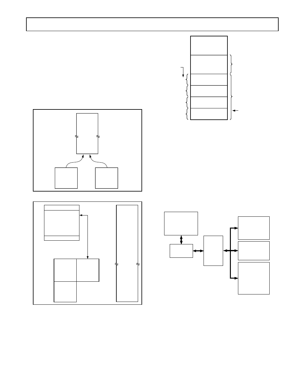
Figure 1. Program and Data Memory Maps
The lower 128 bytes of internal data memory are mapped as
shown in Figure 2. The lowest 32 bytes are grouped into four
banks of eight registers addressed as R0 through R7. The next
16 bytes (128 bits) above the register banks form a block of
bit addressable memory space at bit addresses 00H through 7FH.
BIT-ADDRESSABLE SPACE
(BIT ADDRESSES 0FH–7FH)
4 BANKS OF 8 REGISTERS
R0–R7
BANKS
SELECTED
VIA
BITS IN PSW
11
10
01
00
07H
0FH
17H
1FH
2FH
7FH
00H
08H
10H
18H
20H
RESET VALUE OF
STACK POINTER
Figure 2. Lower 128 Bytes of Internal RAM
MEMORY ORGANIZATION
As with all 8052-compatible devices, the ADuC812 has separate
address spaces for Program and Data memory as shown in Fig-
ure 1. Also as shown in Figure 1, an additional 640 Bytes of
User Data Flash EEPROM are available to the user. The User
Data Flash Memory area is accessed indirectly via a group of
control registers mapped in the Special Function Register (SFR)
area in the Data Memory Space.
The SFR space is mapped in the upper 128 bytes of internal data
memory space. The SFR area is accessed by direct addressing
only and provides an interface between the CPU and all on-chip
peripherals. A block diagram showing the programming model
of the ADuC812 via the SFR area is shown in Figure 3.
128-BYTE
SPECIAL
FUNCTION
REGISTER
AREA
8K BYTE
ELECTRICALLY
REPROGRAMMABLE
NONVOLATILE
FLASH/EE PROGRAM
MEMORY
8051
COMPATIBLE
CORE
OTHER ON-CHIP
PERIPHERALS
TEMPERATURE
SENSOR
2
؋ 12-BIT DACs
SERIAL I/O
PARALLEL I/O
WDT
PSM
AUTO-CALIBRATING
8-CHANNEL
HIGH SPEED
12-BIT ADC
640-BYTE
ELECTRICALLY
REPROGRAMMABLE
NONVOLATILE
FLASH/EE DATA
MEMORY
Figure 3. Programming Model