Using the d/a converter, Aduc812 – Analog Devices ADuC812 User Manual
Page 22
REV. B
ADuC812
–22–
Using the D/A Converter
The on-chip D/A converter architecture consists of a resistor
string DAC followed by an output buffer amplifier, the func-
tional equivalent of which is illustrated in Figure 18. Details of
the actual DAC architecture can be found in U.S. Patent Num-
ber 5969657 (www.uspto.gov). Features of this architecture
include inherent guaranteed monotonicity and excellent differ-
ential linearity.
ADuC812
AV
DD
V
REF
R
R
R
OUTPUT
BUFFER
8
R
R
HIGH-Z
DISABLE
(FROM MCU)
Figure 18. Resistor String DAC Functional Equivalent
As illustrated in Figure 18, the reference source for each DAC is
user selectable in software. It can be either AV
DD
or V
REF.
In
0-to-AV
DD
mode, the DAC output transfer function spans from
0 V to the voltage at the AV
DD
pin. In 0-to-V
REF
mode, the
DAC output transfer function spans from 0 V to the internal
V
REF
or if an external reference is applied the voltage at the V
REF
pin. The DAC output buffer amplifier features a true rail-to-rail
output stage implementation. This means that, unloaded, each
output is capable of swinging to within less than 100 mV of both
AV
DD
and ground. Moreover, the DAC’s linearity specification
(when driving a 10 k
Ω resistive load to ground) is guaranteed
through the full transfer function except codes 0 to 48, and, in
0-to-AV
DD
mode only, codes 3995 to 4095. Linearity degrada-
tion near ground and V
DD
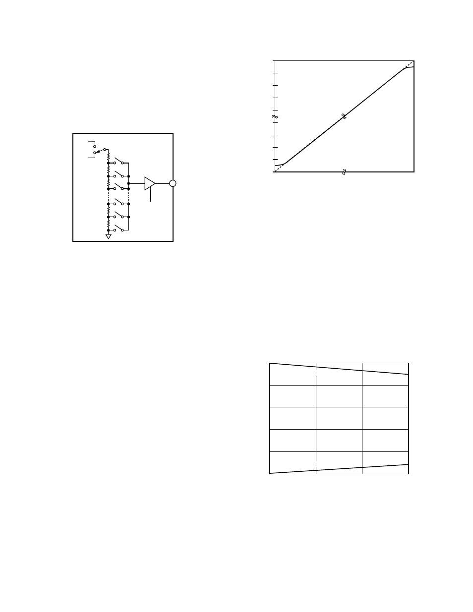
is caused by saturation of the output
amplifier, and a general representation of its effects (neglecting
offset and gain error) is illustrated in Figure 19. The dotted line
in Figure 19 indicates the ideal transfer function, and the solid
line represents what the transfer function might look like with
endpoint nonlinearities due to saturation of the output amplifier.
Note that Figure 19 represents a transfer function in 0-to-V
DD
mode only. In 0-to-V
REF
mode (with V
REF
< V
DD
) the lower
nonlinearity would be similar, but the upper portion of the
transfer function would follow the “ideal” line right to the end
(V
REF
in this case, not V
DD
), showing no signs of endpoint lin-
earity errors.
V
DD
FFF HEX
000 HEX
V
DD
– 50mV
V
DD
– 100mV
100mV
50mV
0mV
Figure 19. Endpoint Nonlinearities Due to Amplifier
Saturation
The endpoint nonlinearities conceptually illustrated in Figure 19
get worse as a function of output loading. Most of the ADuC812’s
data sheet specifications assume a 10 k
Ω resistive load to ground
at the DAC output. As the output is forced to source or sink
more current, the nonlinear regions at the top or bottom
(respectively) of Figure 19 become larger. With larger current
demands, this can significantly limit output voltage swing.
Figure 20 and Figure 21 illustrate this behavior. It should be noted
that the upper trace in each of these figures is only valid for an
output range selection of 0-to-AV
DD
. In 0-to-V
REF
mode, DAC
loading will not cause high-side voltage drops as long as the
reference voltage remains below the upper trace in the correspond-
ing figure. For example, if AV
DD
= 3 V and V
REF
= 2.5 V, the
high-side voltage will not be affected by loads less than 5 mA.
But somewhere around 7 mA the upper curve in Figure 21 drops
below 2.5 V (V
REF
) indicating that at these higher currents the
output will not be capable of reaching V
REF
.
SOURCE/SINK CURRENT – mA
5
0
5
10
15
OUTPUT VOLTAGE
–
V
4
3
2
1
0
DAC LOADED WITH 0FFF HEX
DAC LOADED WITH 0000 HEX
Figure 20. Source and Sink Current Capability with
V
REF
= V
DD
= 5 V