Power consumption, Power-saving modes, Aduc812 – Analog Devices ADuC812 User Manual
Page 42
REV. B
ADuC812
–42–
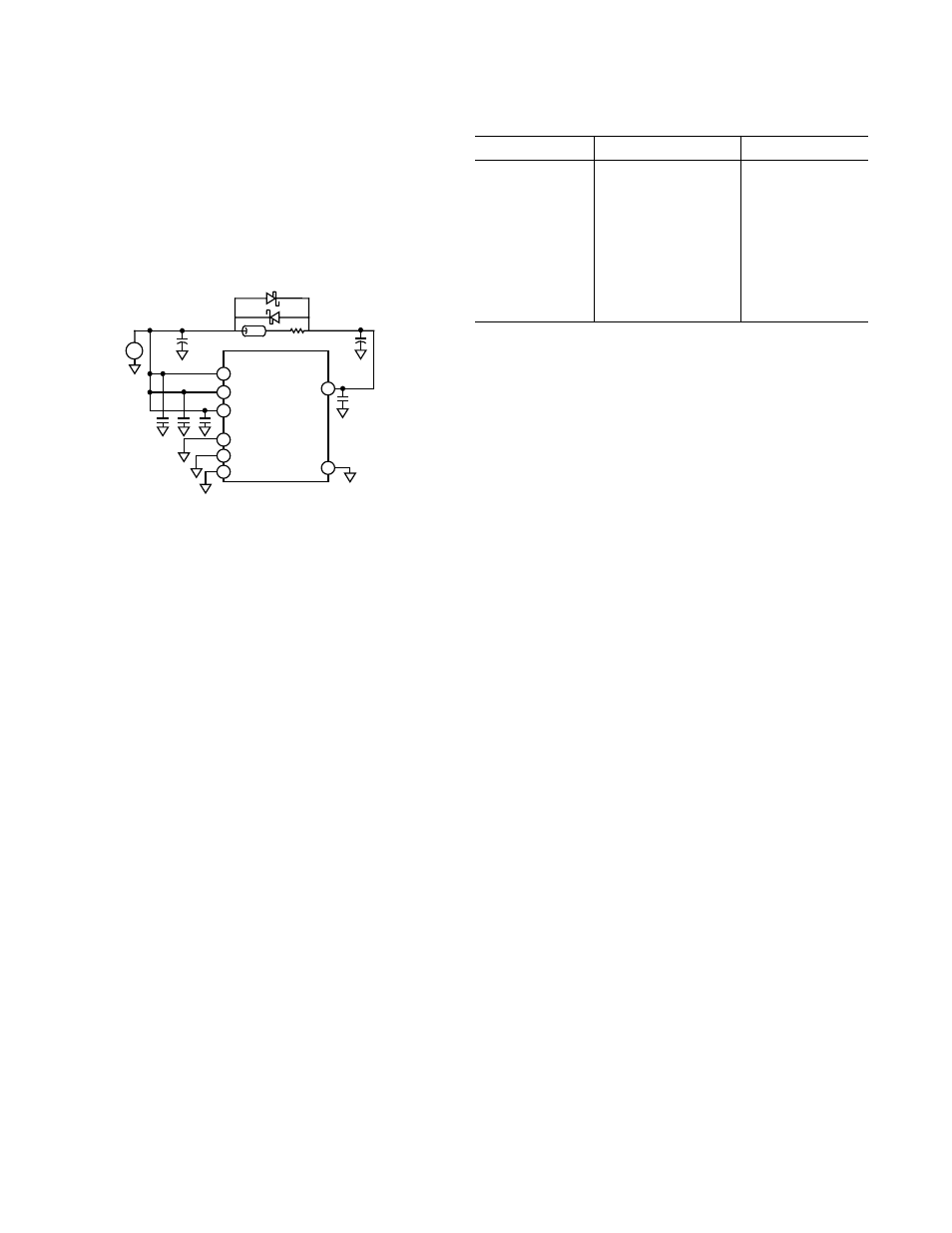
As an alternative to providing two separate power supplies, the
user can help keep AV
DD
quiet by placing a small series resistor
and/or ferrite bead between it and DV
DD
, and then decoupling
AV
DD
separately to ground. An example of this configuration is
shown in Figure 44. With this configuration other analog cir-
cuitry (such as op amps, voltage reference, etc.) can be powered
from the AV
DD
supply line as well. Thne user will still want to
include back-to-back Schottky diodes between AV
DD
and DV
DD
in order to protect from power-up and power-down transient
conditions that could separate the two supply voltages momentarily.
DV
DD
48
34
20
ADuC812
5
6
AGND
AV
DD
0.1
F
10
F
DGND
35
21
47
0.1
F
–
+
DIGITAL SUPPLY
10
F
1.6V
BEAD
Figure 44. External Single-Supply Connections
Notice that in both Figure 43 and Figure 44, a large value (10
µF)
reservoir capacitor sits on DV
DD
and a separate 10
µF capacitor
sits on AV
DD
. Also, local small-value (0.1
µF) capacitors are
located at each V
DD
pin of the chip. As per standard design prac-
tice, be sure to include all of these capacitors, and ensure the
smaller capacitors are close to each AV
DD
pin with trace lengths as
short as possible. Connect the ground terminal of each of these
capacitors directly to the underlying ground plane. Finally, it
should also be noted that, at all times, the analog and digital
ground pins on the ADuC812 must be referenced to the same
system ground reference point.
Power Consumption
The currents consumed by the various sections of the
ADuC812 are shown in Table XXVIII. The “CORE” values
given represent the current drawn by DV
DD
, while the rest
(“ADC,” “DAC,” “voltage ref”) are pulled by the AV
DD
pin
and can be disabled in software when not in use. The other
on-chip peripherals (watchdog timer, power supply monitor,
etc.) consume negligible current and are therefore lumped in
with the “CORE” operating current here. Of course, the user
must add any currents sourced by the parallel and serial I/O
pins, and that sourced by the DAC, in order to determine the
total current needed at the ADuC812’s supply pins. Also,
current drawn from the DV
DD
supply will increase by
approximately 10 mA during Flash/EE erase and program cycles.
Table XXVIII. Typical I
DD
of Core and Peripherals
VDD = 5 V
VDD = 3 V
Core:
(Normal Mode)
(1.6 nAs
× MCLK) + (0.8 nAs × MCLK) +
6 mA
3 mA
Core:
(Idle Mode)
(0.75 nAs
× MCLK) + (0.25 nAs × MCLK) +
5 mA
3 mA
ADC:
1.3 mA
1.0 mA
DAC (Each):
250
µA
200
µA
Voltage Ref:
200
µA
150
µA
Since operating DV
DD
current is primarily a function of clock
speed, the expressions for “CORE” supply current in Table
XXVIII are given as functions of M
CLK
, the oscillator frequency.
Plug in a value for M
CLK
in hertz to determine the current con-
sumed by the core at that oscillator frequency. Since the ADC
and DACs can be enabled or disabled in software, add only the
currents from the peripherals you expect to use. The internal
voltage reference is automatically enabled whenever either the
ADC or at least one DAC is enabled. And again, do not forget
to include current sourced by I/O pins, serial port pins, DAC
outputs, etc., plus the additional current drawn during Flash/EE
erase and program cycles.
A software switch allows the chip to be switched from normal
mode into idle mode, and also into full power-down mode. Below
are brief descriptions of power-down and idle modes.
In idle mode, the oscillator continues to run, but is gated off to
the core only. The on-chip peripherals continue to receive the
clock, and remain functional. Port pins and DAC output pins
retain their states in this mode. The chip will recover from idle
mode upon receiving any enabled interrupt, or on receiving a
hardware reset.
In full power-down mode, the on-chip oscillator stops, and all
on-chip peripherals are shut down. Port pins retain their logic
levels in this mode, but the DAC output goes to a high-impedance
state (three-state). The chip will only recover from power-down
mode upon receiving a hardware reset or when power is cycled.
During full power-down mode, the ADuC812 consumes a total
of approximately 5
µA.