Grounding and board layout recommendations, Aduc812 – Analog Devices ADuC812 User Manual
Page 43
REV. B
ADuC812
–43–
Grounding and Board Layout Recommendations
As with all high resolution data converters, special attention must
be paid to grounding and PC board layout of ADuC812-based
designs in order to achieve optimum performance from the ADCs
and DAC.
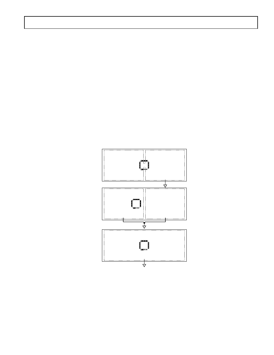
Although the ADuC812 has separate pins for analog and digital
ground (AGND and DGND), the user must not tie these to two
separate ground planes unless the two ground planes are con-
nected together very close to the ADuC812, as illustrated in the
simplified example of Figure 45a. In systems where digital and
analog ground planes are connected together somewhere else
(at the system’s power supply for example), they cannot be con-
nected again near the ADuC812 since a ground loop would result.
In these cases, tie the ADuC812’s AGND and DGND pins all
to the analog ground plane, as illustrated in Figure 45b. In systems
with only one ground plane, ensure that the digital and analog
components are physically separated onto separate halves of the
board such that digital return currents do not flow near analog
circuitry and vice versa. The ADuC812 can then be placed between
the digital and analog sections, as illustrated in Figure 45c.
In all of these scenarios, and in more complicated real-life appli-
cations, keep in mind the flow of current from the supplies and
back to ground. Make sure the return paths for all currents are
as close as possible to the paths the currents took to reach their
destinations. For example, do not power components on the
analog side of Figure 45b with DV
DD
since that would force
return currents from DV
DD
to flow through AGND. Also, try to
avoid digital currents flowing under analog circuitry, which could
happen if the user placed a noisy digital chip on the left half
of the board in Figure 45c. Whenever possible, avoid large
discontinuities in the ground plane(s) (such as are formed by a
long trace on the same layer), since they force return signals to
travel a longer path. And of course, make all connections to the
ground plane directly, with little or no trace separating the pin
from its via to ground.
If the user plans to connect fast logic signals (rise/fall time < 5 ns)
to any of the ADuC812’s digital inputs, add a series resistor to
each relevant line to keep rise and fall times longer than 5 ns at
the ADuC812 input pins. A value of 100
Ω or 200 Ω is usually
sufficient to prevent high-speed signals from coupling capacitively
into the ADuC812 and affecting the accuracy of ADC conversions.
B
DGND
AGND
PLACE ANALOG
COMPONENTS
HERE
PLACE DIGITAL
COMPONENTS
HERE
C
GND
PLACE ANALOG
COMPONENTS
HERE
PLACE DIGITAL
COMPONENTS
HERE
DGND
AGND
PLACE ANALOG
COMPONENTS HERE
A
PLACE DIGITAL
COMPONENTS HERE
Figure 45. System Grounding Schemes