Aduc812 – Analog Devices ADuC812 User Manual
Page 51
REV. B
ADuC812
–51–
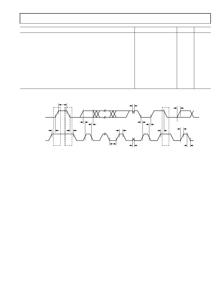
Parameter
Min
Max
Unit
Figure
I
2
C-COMPATIBLE INTERFACE TIMING
t
L
SCLOCK Low Pulsewidth
4.7
µs
56
t
H
SCLOCK High Pulsewidth
4.0
µs
56
t
SHD
Start Condition Hold Time
0.6
µs
56
t
DSU
Data Setup Time
100
ns
56
t
DHD
Data Hold Time
0
0.9
µs
56
t
RSU
Setup Time for Repeated Start
0.6
µs
56
t
PSU
Stop Condition Setup Time
0.6
µs
56
t
BUF
Bus Free Time between a STOP
Condition and a START Condition
1.3
µs
56
t
R
Rise Time of Both SCLOCK and SDATA
300
ns
56
t
F
Fall Time of Both SCLOCK and SDATA
300
ns
56
t
SUP
1
Pulsewidth of Spike Suppressed
50
ns
56
NOTE
1
Input filtering on both the SCLOCK and SDATA inputs suppress noise spikes which are less than 50 ns.
SDATA (I/O)
SCLK (I)
STOP
CONDITION
START
CONDITION
PS
REPEATED
START
S(R)
1
2-7
8
9
1
MSB
t
BUF
t
DSU
t
DHD
t
SHD
t
PSU
t
H
t
SUP
t
L
t
SUP
t
DSU
t
DHD
t
RSU
t
R
t
R
t
F
LSB
ACK
MSB
Figure 55. I
2
C-Compatible Interface Timing