Timing specifications, Aduc812 – Analog Devices ADuC812 User Manual
Page 46
REV. B
ADuC812
–46–
(AV
DD
= DV
DD
= 3.0 V or 5.0 V
؎ 10%. All specifications T
A
= T
MIN
to T
MAX
unless otherwise noted.)
12 MHz
Variable Clock
Parameter
Min
Typ
Max
Min
Typ
Max
Unit
Figure
CLOCK INPUT (External Clock Driven XTAL1)
t
CK
XTAL1 Period
83.33
62.5
1000
ns
50
t
CKL
XTAL1 Width Low
20
20
ns
50
t
CKH
XTAL1 Width High
20
20
ns
50
t
CKR
XTAL1 Rise Time
20
20
ns
50
t
CKF
XTAL1 Fall Time
20
20
ns
50
t
CYC
4
ADuC812 Machine Cycle Time
1
12t
CK
µs
NOTES
1
AC inputs during testing are driven at DV
DD
– 0.5 V for a Logic 1 and 0.45 V for a Logic 0. Timing measurements are made at V
IH
min for a Logic 1 and V
IL
max for
a Logic 0.
2
For timing purposes, a port pin is no longer floating when a 100 mV change from load voltage occurs. A port pin begins to float when a 100 mV change from the
loaded V
OH
/V
OL
level occurs.
3
C
LOAD
for Port0, ALE,
PSEN outputs = 100 pF; C
LOAD
for all other outputs = 80 pF unless otherwise noted.
4
ADuC812 Machine Cycle Time is nominally defined as MCLKIN/12.
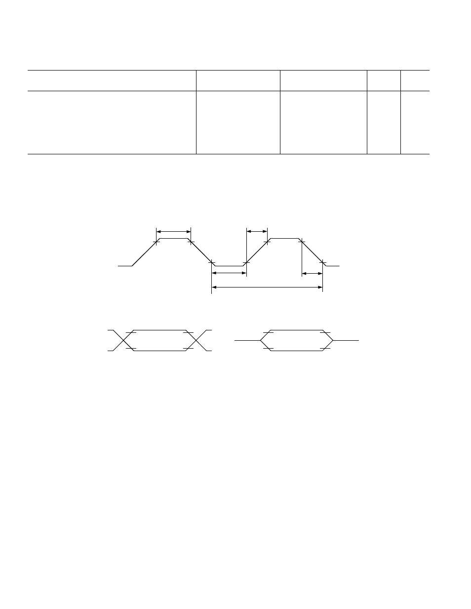
t
CKL
t
CKF
t
CK
t
CKH
t
CKR
Figure 49. XTAL 1 Input
DV
DD
– 0.5V
0.45V
0.2V
CC
+ 0.9V
TEST POINTS
0.2V
CC
– 0.1V
V
LOAD
– 0.1V
V
LOAD
V
LOAD
+ 0.1V
TIMING
REFERENCE
POINTS
V
LOAD
– 0.1V
V
LOAD
V
LOAD
– 0.1V
Figure 50. Timing Waveform Characteristics
TIMING SPECIFICATIONS
1, 2, 3