Analog Devices ADuC812 User Manual
Aduc812, Microconverter, Multichannel 12-bit adc with embedded flash mcu

REV. B
Information furnished by Analog Devices is believed to be accurate and
reliable. However, no responsibility is assumed by Analog Devices for its
use, nor for any infringements of patents or other rights of third parties that
may result from its use. No license is granted by implication or otherwise
under any patent or patent rights of Analog Devices.
a
ADuC812
One Technology Way, P.O. Box 9106, Norwood, MA 02062-9106, U.S.A.
Tel: 781/329-4700
Fax: 781/326-8703
© Analog Devices, Inc., 2001
MicroConverter
®
, Multichannel
12-Bit ADC with Embedded FLASH MCU
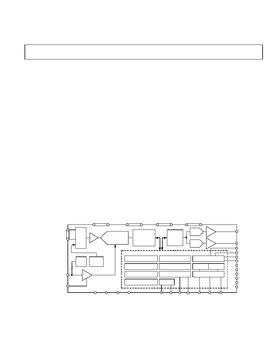
FUNCTIONAL BLOCK DIAGRAM
MICROCONTROLLER
8051 BASED
MICROCONTROLLER CORE
POWER SUPPLY
MONITOR
WATCHDOG
TIMER
2-WIRE
SERIAL I/O
640
؋ 8 USER
FLASH EEPROM
256
؋ 8 USER
RAM
SPI
12-BIT
SUCCESSIVE
APPROXIMATION
ADC
ADC
CONTROL
AND
CALIBRATION
LOGIC
T/H
TEMP
SENSOR
2.5V
REF
AIN
MUX
BUF
DAC0
MOSI/
SDATA
MISO
(P3.3)
SCLOCK
TxD
(P3.1)
RxD
(P3.0)
XTAL2
XTAL1
DGND
DV
DD
AGND
AV
DD
DAC0
DAC1
T0 (P3.4)
T1 (P3.5)
T2 (P1.0)
T2EX (P1.1)
INT0 (P3.2)
INT1 (P3.3)
ALE
PSEN
EA
RESET
ADuC812
P3.0–P3.7
P2.0–P2.7
P1.0–P1.7
P0.0–P0.7
AIN0 (P1.0)–AIN7 (P1.7)
V
REF
UART
8K
؋ 8 PROGRAM
FLASH EEPROM
DAC
CONTROL
3
؋ 16-BIT
TIMER/COUNTERS
OSC
MUX
DAC1
BUF
C
REF
BUF
FEATURES
ANALOG I/O
8-Channel, High Accuracy 12-Bit ADC
On-Chip, 100 ppm/
؇C Voltage Reference
High-Speed 200 kSPS
DMA Controller for High-Speed ADC-to-RAM Capture
Two 12-Bit Voltage Output DACs
On-Chip Temperature Sensor Function
MEMORY
8K Bytes On-Chip Flash/EE Program Memory
640 Bytes On-Chip Flash/EE Data Memory
256 Bytes On-Chip Data RAM
16M Bytes External Data Address Space
64K Bytes External Program Address Space
8051-COMPATIBLE CORE
12 MHz Nominal Operation (16 MHz Max)
Three 16-Bit Timer/Counters
High Current Drive Capability—Port 3
Nine Interrupt Sources, Two Priority Levels
POWER
Specified for 3 V and 5 V Operation
Normal, Idle, and Power-Down Modes
ON-CHIP PERIPHERALS
UART Serial I/O
2-Wire (I
2
C
®
-Compatible) and SPI
®
Serial I/O
Watchdog Timer
Power Supply Monitor
APPLICATIONS
Intelligent Sensors Calibration and Conditioning
Battery Powered Systems (Portable PCs, Instruments,
Monitors)
Transient Capture Systems
DAS and Communications Systems
Control Loop Monitors (Optical Networks/Base Stations)
GENERAL DESCRIPTION
The ADuC812 is a fully integrated 12-bit data acquisition system
incorporating a high performance self calibrating multichannel
ADC, dual DAC and programmable 8-bit MCU (8051 instruc-
tion set compatible) on a single chip.
The programmable 8051-compatible core is supported by 8K
bytes Flash/EE program memory, 640 bytes Flash/EE data
memory and 256 bytes data SRAM on-chip.
Additional MCU support functions include Watchdog Timer,
Power Supply Monitor and ADC DMA functions. 32 Pro-
grammable I/O lines, I
2
C-compatible, SPI and Standard UART
Serial Port I/O are provided for multiprocessor interfaces and
I/O expansion.
Normal, idle, and power-down operating modes for both the
MCU core and analog converters allow for flexible power man-
agement schemes suited to low power applications. The part is
specified for 3 V and 5 V operation over the industrial tem-
perature range and is available in a 52-lead, plastic quad
flatpack package.
MicroConverter is a registered trademark of Analog Devices, Inc.
I
2
C is a registered trademark of Philips Corporation.
SPI is a registered trademark of Motorola Inc.
Document Outline
- FEATURES
- GENERAL DESCRIPTION
- SPECIFICATIONS
- ABSOLUTE MAXIMUM RATINGS
- ORDERING GUIDE
- PIN FUNCTION DESCRIPTIONS
- TERMINOLOGY
- ADC SPECIFICATIONS
- DAC SPECIFICATIONS
- ARCHITECTURE, MAIN FEATURES
- MEMORY ORGANIZATION
- OVERVIEW OF MCU-RELATED SFRs
- SPECIAL FUNCTION REGISTERS
- ADC CIRCUIT INFORMATION
- General Overview
- ADC Transfer Function
- Typical Operation
- ADCCON1 — (ADC Control SFR #1)
- ADCCON2 — (ADC Control SFR #2)
- ADCCON3 — (ADC Control SFR #3)
- Driving the A/D Converter
- Voltage Reference Connections
- Configuring the ADC
- ADC DMA Mode
- Micro Operation During the ADC DMA Mode
- The Offset and Gain Calibration Coefficients
- Calibration
- NONVOLATILE FLASH MEMORY
- USER INTERFACE TO OTHER ON-CHIP ADuC812 PERIPHERALS
- WATCHDOG TIMER
- POWER SUPPLY MONITOR
- SERIAL PERIPHERAL INTERFACE
- I2C COMPATIBLE INTERFACE
- 8051-COMPATIBLE ON-CHIP PERIPHERALS
- TIMER/COUNTER 0 AND 1 OPERATING MODES
- UART SERIAL INTERFACE
- INTERRUPT SYSTEM
- ADuC812 HARDWARE DESIGN CONSIDERATIONS
- OTHER HARDWARE CONSIDERATIONS
- QUICKSTART DEVELOPMENT SYSTEM
- TIMING SPECIFICATIONS
- OUTLINE DIMENSIONS
- Revision History
