Serial peripheral interface, Miso (master in, slave out data i/o pin), pin #19, Mosi (master out, slave in pin), pin #27 – Analog Devices ADuC812 User Manual
Page 26: Sclock (serial clock i/o pin), pin #26, Ss (slave select input pin), pin #12, Aduc812
REV. B
ADuC812
–26–
SERIAL PERIPHERAL INTERFACE
The ADuC812 integrates a complete hardware Serial Peripheral
Interface (SPI) on-chip. SPI is an industry standard synchronous
serial interface that allows eight bits of data to be synchronously
transmitted and received simultaneously, i.e., full duplex.
It should be noted that the SPI pins are shared with the I
2
C
interface and therefore the user can only enable one or the other
interface at any given time (see SPE in SPICON below).
The SPI Port can be configured for Master or Slave operation and
typically consists of four pins, namely:
MISO (Master In, Slave Out Data I/O Pin), Pin #19
The MISO (master in slave out) pin is configured as an input line
in master mode and an output line in slave mode. The MISO
line on the master (data in) should be connected to the MISO
line in the slave device (data out). The data is transferred as
byte wide (8-bit) serial data, MSB first.
MOSI (Master Out, Slave In Pin), Pin #27
The MOSI (master out slave in) pin is configured as an output line
in master mode and an input line in slave mode. The MOSI
line on the master (data out) should be connected to the MOSI
line in the slave device (data in). The data is transferred as byte
wide (8-bit) serial data, MSB first.
SCLOCK (Serial Clock I/O Pin), Pin #26
The master serial clock (SCLOCK) is used to synchronize
the data being transmitted and received through the MOSI
and MISO data lines. A single data bit is transmitted and
received in each SCLOCK period. Therefore, a byte is
transmitted/received after eight SCLOCK periods. The
SCLOCK pin is configured as an output in master mode and as
an input in slave mode. In master mode the bit-rate, polarity
and phase of the clock are controlled by the CPOL, CPHA,
SPR0 and SPR1 bits in the SPICON SFR (see Table XII).
In slave mode the SPICON register will have to be configured
with the phase and polarity (CPHA and CPOL) of the expected
input clock. In both master and slave mode the data is transmitted
on one edge of the SCLOCK signal and sampled on the other. It
is important therefore that the CPHA and CPOL are configured the
same for the master and slave devices.
SS (Slave Select Input Pin), Pin #12
The Slave Select (
SS) input pin is shared with the ADC5 input.
In order to configure this pin as a digital input the bit must be
cleared, e.g., CLR P1.5.
This line is active low. Data is only received or transmitted in
slave mode when the
SS pin is low, allowing the ADuC812 to
be used in single master, multislave SPI configurations. If
CPHA = 1 then the
SS input may be permanently pulled low.
With CPHA = 0 then the
SS input must be driven low before
the first bit in a byte wide transmission or reception and return
high again after the last bit in that byte wide transmission or
reception. In SPI Slave Mode, the logic level on the external
SS
pin (Pin #13), can be read via the SPR0 bit in the SPICON SFR.
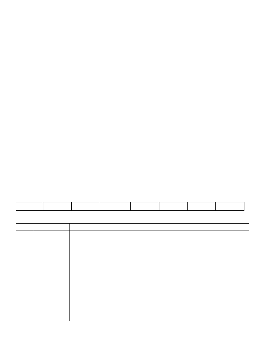
The following SFR registers are used to control the SPI interface.
SPICON
SPI Control Register
SFR Address
F8H
Power-On Default Value
OOH
Bit Addressable
Yes
I
P
S
I
L
O
C
W
E
P
S
M
I
P
S
L
O
P
C
A
H
P
C
1
R
P
S
0
R
P
S
Table XI. SPICON SFR Bit Designations
Bit
Name
Description
7
ISPI
SPI Interrupt Bit.
Set by MicroConverter at the end of each SPI transfer.
Cleared directly by user code or indirectly by reading the SPIDAT SFR
6
WCOL
Write Collision Error Bit.
Set by MicroConverter if SPIDAT is written to while an SPI transfer is in progress.
Cleared by user code.
5
SPE
SPI Interface Enable Bit.
Set by user to enable the SPI interface.
Cleared by user to enable the I
2
C interface.
4
SPIM
SPI Master/Slave Mode Select Bit.
Set by user to enable Master Mode operation (SCLOCK is an output).
Cleared by user to enable Slave Mode operation (SCLOCK is an input).
3
CPOL
Clock Polarity Select Bit.
Set by user if SCLOCK idles high.
Cleared by user if SCLOCK idles low.
2
CPHA
Clock Phase Select Bit.
Set by user if leading SCLOCK edge is to transmit data.
Cleared by user if trailing SCLOCK edge is to transmit data.