2 × 12a digital dual microdlynx, Non-isolated dc-dc power modules, Datasheet – GE Industrial Solutions 2 × 12A Digital Dual Output MicroDLynx User Manual
Page 4: Electrical specifications, General specifications, Feature specifications
GE
Datasheet
2 × 12A Digital Dual MicroDlynx
TM
: Non-Isolated DC-DC Power Modules
4.5Vdc –14.4Vdc input; 0.51Vdc to 5.5Vdc output; 2 × 12AOutput Current
February 14, 2014
©2014 General Electric Corporation. All rights reserved.
Page 4
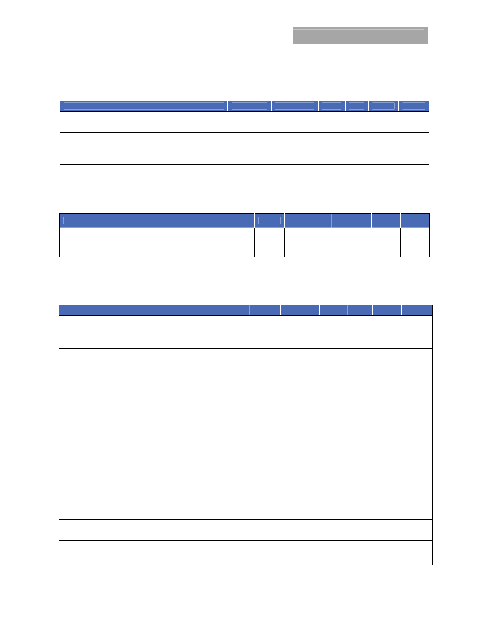
Electrical Specifications
(continued)
Parameter
Device
Symbol
Min
Typ
Max
Unit
Frequency Synchronization
All
Synchronization Frequency Range
All
-20%
+20%
kHz
High-Level Input Voltage
All
VIH
2.0
V
Low-Level Input Voltage
All
VIL
0.4
V
Input Current, SYNC
All
ISYNC
100
nA
Minimum Pulse Width, SYNC
All
tSYNC
100
ns
Maximum SYNC rise time
All
tSYNC_SH
100
ns
General Specifications
Parameter
Device
Min
Typ
Max
Unit
Calculated MTBF (I
O
=0.8I
O, max
, T
A
=40°C) Telecordia Issue 2 Method 1 Case 3
All
75,767,425
Hours
Weight
⎯
4.5 (0.16)
⎯
g (oz.)
Feature Specifications
Unless otherwise indicated, specifications apply over all operating input voltage, resistive load, and temperature conditions. See
Feature Descriptions for additional information.
Parameter
Device
Symbol
Min
Typ
Max
Unit
On/Off Signal Interface
(V
IN
=V
IN, min
to V
IN, max
; open collector or equivalent,
Signal referenced to GND)
Device Code with no suffix – Negative Logic (See Ordering Information)
(On/OFF pin is open collector/drain logic input with
external pull-up resistor; signal referenced to GND)
Logic High (Module OFF)
Input High Current
All
I
IH1,
I
IH2
— — 1 mA
Input High Voltage
All
V
IH1,
V
IH2
2 —
V
IN, max
Vdc
Logic Low (Module ON)
Input low Current
All
I
IL1,
I
IL2
— — 20 μA
Input Low Voltage
All
V
IL1,
V
IL2
-0.2 — 0.6 Vdc
Turn-On Delay and Rise Times
(V
IN
=V
IN, nom
, I
O
=I
O, max ,
V
O
to within ±1% of steady state)
Case 1: On/Off input is enabled and then input power is
applied (delay from instant at which V
IN
= V
IN, min
until V
o
=
10% of V
o, set
)
All
Tdelay1,
Tdelay2
— 2 — msec
Case 2: Input power is applied for at least one second and
then the On/Off input is enabled (delay from instant at
which Von/Off is enabled until V
o
= 10% of V
o, set
)
All
Tdelay1,
Tdelay2
— 800 — μsec
Output voltage Rise time (time for V
o
to rise from
10% of Vo, set to 90% of Vo, set)
All Trise1,
Trise2
— 5 — msec
Output voltage overshoot (T
A
= 25
o
C
V
IN
= V
IN, min
to V
IN, max
,I
O
= I
O, min
to I
O, max
)
With or without maximum external capacitance
Both
Outputs
3.0
%
V
O, set