4v (figure 25) – Rainbow Electronics MAX1329 User Manual
Page 71
MAX1329/MAX1330
12-/16-Bit DASs with ADC, DACs, DPIOs, APIOs,
Reference, Voltage Monitors, and Temp Sensor
______________________________________________________________________________________
71
Charge-Pump Component Selection
Optimize the charge-pump circuit for size, quiescent
current, and output ripple by properly selecting the
operating frequency and capacitors C
DVDD
, C
FLY
, and
C
AVDD
(Table 32). The charge pump is capable of pro-
viding a maximum of 25mA including what is used
internally. If less than 25mA is required, smaller capaci-
tor values can be utilized.
For lowest ripple, select 117kHz operation (CPDIV<1:0>
= 00 and OSCE = 1 when using the internal oscillator). In
addition, increasing C
AVDD
relative to C
FLY
further
reduces ripple. For highest efficiency, select 14.6kHz
operation (CPDIV<1:0> = 11 and OSCE = 1 when using
the internal oscillator) and select the largest practical
values for C
AVDD
and C
FLY
while maintaining at least a
30-to-1 ratio. For smallest size, select 117kHz operation.
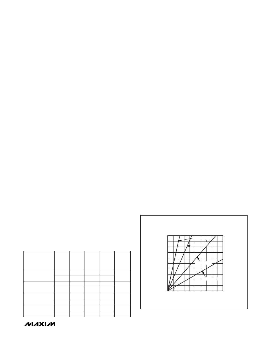
See Table 32 for some suggested values and resulting
ripple for 25mA load current. See Figure 34 for load cur-
rent vs. flying capacitor value when optimizing for other
load currents.
Note that the capacitors must have low ESR to main-
tain low ripple. The C
FLY
flying capacitor ESR needs
to be < 0.1Ω; and the C
AVDD
and C
DVDD
filter capaci-
tor ESR needs to be < 0.3Ω. The C
FLY
flying capacitor
can easily be a ceramic capacitor; and the C
AVDD
and
C
DVDD
filter capacitor can be a low-ESR tantalum or
may need to be a combination of a small ceramic and a
larger tantalum capacitor.
When DV
DD
is lower than AV
DD
, the charge pump always
operates in voltage-doubler mode. It regulates the output
voltage using a pulse-width-modulation (PWM) scheme.
Using a PWM scheme ensures that the charge pump is
synchronous with the internal ADC preventing corruption
of the conversion results.
Operating the Analog Switches
The MAX1329/MAX1330 include two single-pole double-
throw (SPDT) and three single-pole single-throw (SPST)
analog switches. The two SPDT analog switches are
uncommitted and the three SPST analog switches are
connected between the DAC buffer or op amp outputs
and the inverting inputs.
The analog switches can be controlled using the Switch
Control register or any of the DPIOs. See the DPIO
Control and DPIO Setup registers to program the
DPIOs. The DPIOs should be used when direct control
is critical such as synchronizing with another event or if
the SPI bus bandwidth is not sufficient for the intended
application. The register bit for the analog switch is log-
ically OR’d with DPIOs enabled to control that switch.
The SPDT1 and SPDT2 analog switches can be operat-
ed as a SPDT or as a double-pole single-throw (DPST).
In the DPST mode, both switches can be opened or
closed together. This is useful when connecting two
external nodes to a common point. If a lower on-resis-
tance is required, NO_ and NC_ can be connected
together externally and be used as a SPST analog
switch with half the on-resistance.
The SPST analog switches are intended to be used to
set the DAC buffers and op amps to unity gain internal-
ly by software control. When the DAC buffers and op
amps are used as transimpedance amplifiers, the SPST
analog switches can be used to short the external tran-
simpedance resistor during high current periods to
keep the amplifier output in compliance.
CHARGE-PUMP
CLOCK (kHz)
I
LOAD,
MAX
(mA)
C
FLY
(µF)
C
AVDD
(µF)
C
DVDD
(µF)
RIPPLE
(mV)
25
1.7
55.6
17.4
14.4
12.5
0.9
27.8
8.7
32
25
0.9
27.8
8.7
28.8
12.5
0.4
13.9
4.3
32
25
0.4
13.9
4.3
57.6
12.5
0.2
6.9
2.2
32
25
0.2
6.9
2.2
115.2
12.5
0.1
3.5
1.1
32
Table 32. External Component Selection
for 25mA Output Current and 2V
DVDD
-
V
AVDD
≥ 0.4V (Figure 25)
CHARGE-PUMP LOAD CURRENT
vs. FLYING CAPACITOR VALUE
MAX1329 fig34
C
FLY
(µF)
I
LOAD (mA)
4.5
4.0
3.0 3.5
1.0 1.5 2.0 2.5
0.5
5
10
15
20
25
30
35
40
45
50
0
0
5.0
f
CP
= 115.2kHz
f
CP
= 57.6kHz
f
CP
= 14.4kHz
f
CP
= 28.8kHz
Figure 34. Load Current vs. CFLY Value for 2V
DVDD
- V
AVDD
≥ 0.4V