Pin description (continued) – Rainbow Electronics MAX1329 User Manual
Page 24
MAX1329/MAX1330
12-/16-Bit DASs with ADC, DACs, DPIOs, APIOs,
Reference, Voltage Monitors, and Temp Sensor
24
______________________________________________________________________________________
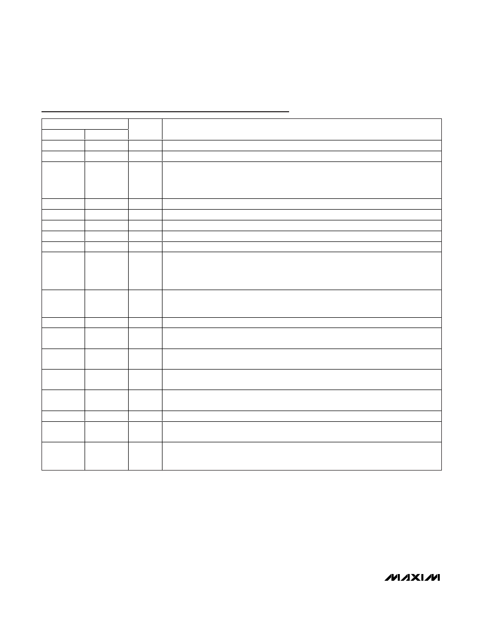
Pin Description (continued)
PIN
MAX1329
MAX1330
NAME
FUNCTION
24
24
OUTA
DACA Force-Sense Output. Also internally connected to ADC mux.
25
25
FBA
DACA Force-Sense Feedback Input. Also internally connected to ADC mux.
26
26
REFDAC
DAC Internal Reference Buffer Output/DAC External Reference Input. In internal reference
mode, REFDAC provides a 1.25V, 2.048V, or 2.5V internal reference buffer output. In
external DAC reference buffer mode, disable internal reference buffer. Bypass REFDAC to
AGND with a 1µF capacitor.
27
27
SNC2
Analog Switch 2 Normally-Closed Terminal
28
28
SCM2
Analog Switch 2 Common Terminal
29
29
SNO2
Analog Switch 2 Normally-Open Terminal
30
30
AIN2
Analog Input 2. Also internally connected to ADC mux.
31
31
AIN1
Analog Input 1. Also internally connected to ADC mux.
32
32
REFADC
ADC Internal Reference Buffer Output/ADC External Reference Input. In internal reference
mode, REFADC provides a 1.25V, 2.048V, or 2.5V internal reference buffer output. In
external ADC reference buffer mode, disable internal reference buffer. Bypass REFADC to
AGND with a 1µF capacitor.
33
33
REFADJ
Internal Reference Output/Reference Buffer Amplifiers Input. In internal reference mode,
bypass REFADJ to AGND with a 0.01µF capacitor. In external reference mode, disable
internal reference.
34
34
AGND
Analog Ground
35
35
AV
DD
Analog Supply Input. Bypass AV
DD
to AGND with at least a 0.01µF capacitor. With the
charge pump enabled, see Table 32 for required capacitor values.
36
36
C1B
Charge-Pump Capacitor Input B. Connect C
FLY
across C1A and C1B. See Table 32 for
required capacitor values.
37
37
C1A
Charge-Pump Capacitor Input A. Connect C
FLY
across C1A and C1B. See Table 32 for
required capacitor values.
38
38
DV
DD
Digital Supply Input. Bypass DV
DD
to DGND with at least a 0.01µF capacitor. When using
charge pump, see Table 32 for required capacitor values.
39
39
DGND
Digital Ground
40
40
CLKIO
Clock Input/Output. In internal clock mode, enable CLKIO output for external use. In
external clock mode, apply a clock signal at CLKIO for the ADC and charge pump.
—
—
EP
Exposed Pad. The exposed pad is located on the package bottom and is internally
connected to AGND. Connect EP to the analog ground plane. Do not route any PCB traces
under the package.