Absolute maximum ratings, Electrical characteristics – Rainbow Electronics MAX1329 User Manual
Page 2
MAX1329/MAX1330
12-/16-Bit DASs with ADC, DACs, DPIOs, APIOs,
Reference, Voltage Monitors, and Temp Sensor
2
_______________________________________________________________________________________
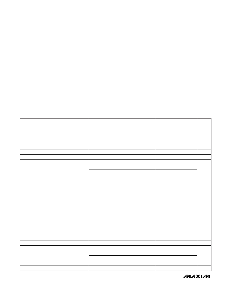
ABSOLUTE MAXIMUM RATINGS
Stresses beyond those listed under “Absolute Maximum Ratings” may cause permanent damage to the device. These are stress ratings only, and functional
operation of the device at these or any other conditions beyond those indicated in the operational sections of the specifications is not implied. Exposure to
absolute maximum rating conditions for extended periods may affect device reliability.
AV
DD
to AGND .........................................................-0.3V to +6V
DV
DD
to DGND.........................................................-0.3V to +6V
Analog Inputs to AGND....................................-0.3V to the lower
of (AV
DD
+ 0.3V) or +6V
Digital Inputs to DGND.....................................-0.3V to the lower
of (
DV
DD
+ 0.3V) or +6V
Analog Outputs to AGND .................................-0.3V to the lower
of (AV
DD
+ 0.3V) or +6V
Digital Outputs to DGND ..................................-0.3V to the lower
of (DV
DD
+ 0.3V) or 6V
AGND to DGND.................................................... -0.3V to +0.3V
Continuous Current into Any Pin.......................................±50mA
Continuous Power Dissipation (T
A
= +70°C)
40-Pin Thin QFN (derate 37mW/°C above +70°C) ....2963mW
Operation Temperature Range............................-40°C to +85°C
Storage Temperature Range .............................-65°C to +150°C
Junction Temperature ......................................................+150°C
Lead Temperature (soldering, 10s) ................................+300°C
ELECTRICAL CHARACTERISTICS
(DV
DD
= 1.8V to 3.6V, AV
DD
= 2.7V to 5.5V, V
REFDAC
= V
REFADC
= 2.5V, external reference; 10µF capacitor at REFADC and REFDAC;
0.01µF capacitor at REFADJ; T
A
= T
MIN
to T
MAX
, unless otherwise noted. Typical values are at T
A
= +25°C.)
PARAMETER
SYMBOL
CONDITIONS
MIN
TYP
MAX
UNITS
ADC
Resolution
No missing codes
12
Bits
DSP-Mode Resolution
256 oversampling, dither enabled
16
Bits
Integral Nonlinearity
INL
Normal mode (Note 1)
±1
LSB
12
Differential Nonlinearity
DNL
Normal mode (Note 1)
±1
LSB
12
Offset Error
(Note 1)
±4
mV
Offset Drift
±1.5
µV/°C
Gain = 1
±0.1
Gain = 2, 4
±1.5
Gain Error (Excluding Reference)
(Note 1)
Gain = 8
±2.5
% FS
Gain Temperature Coefficient
Excluding reference
±0.8
ppm/°C
Unipolar mode, gain = 1, 2, 4, 8
0
+ V
R E F AD C
/
Gain
Voltage Range
Bipolar mode, gain = 1, 2, 4, 8
-V
REFADC
/
(2 x Gain)
+ V
R E F AD C
/
(2 x Gain)
V
Absolute Input Voltage Range
AGND
AV
DD
V
Input Leakage Current into
Analog Inputs
(Note 2)
±0.5
±1
nA
Gain = 1, 2
24
Input Capacitance
Gain = 4, 8
48
pF
Gain = 1, 2
0.6
Acquisition Time
t
ACQ
Gain = 4, 8
1.2
µs
Conversion Time
t
CONV
12 clocks
2.4
µs
Conversion Clock Frequency
0.1
5.0
MHz
Normal operation mode,
ADC converting at 234ksps
325
ADC Supply Current (Note 3)
Fast power-down mode,
ADC converting at 234ksps
210
µA
Aperture Delay
t
AD
30
ns