Table 20. adc acquisition clock bit configuration – Rainbow Electronics MAX1329 User Manual
Page 53
MAX1329/MAX1330
12-/16-Bit DASs with ADC, DACs, DPIOs, APIOs,
Reference, Voltage Monitors, and Temp Sensor
______________________________________________________________________________________
53
CP/VM Control Register
The CP/VM (Charge Pump/Voltage Monitor) Control
register configures the interrupt polarity, charge-pump
output voltage settings and power-down, supply volt-
age bypass switch state, and the voltage monitor set-
tings for DV
DD
and AV
DD
.
INTP: Interrupt Polarity bit (default = 0). INTP controls
the output polarity for
RST1 and RST2 when configured
as interrupt outputs. INTP = 0 results in active-low oper-
ation and INTP = 1 selects active-high operation.
VM1<1:0>: Voltage Monitor 1 (VM1) Control bits
(default = 00). VM1 monitors the voltage on DV
DD
. The
VM1<1:0> bits control the threshold and output settings
of VM1 (see Table 21).
RST1 and RST2 are open-drain
outputs when configured as voltage monitor outputs
and are push-pull when configured as interrupt outputs.
The VM1A status bit is set when DV
DD
drops below the
1.8V threshold and the VM1B status bit is set when
DV
DD
drops below the 2.7V threshold.
VM2CP<2:0>: Voltage Monitor 2 (VM2) and Charge-
Pump Control bits (default = 000). VM2CP<2:0> control
the charge pump, the bypass switch, and the AV
DD
volt-
age monitor. The charge pump generates a regulated
AV
DD
supply voltage from a DV
DD
input. When activated
(VM2CP = 100), the bypass switch internally shorts
DV
DD
to AV
DD
. VM2 monitors the voltage on AV
DD
and
sets the VM2 Status bit when AV
DD
drops below
the threshold.
CPDIV<1:0>: Charge-Pump Clock Divider bits (default =
00). The CPDIV<1:0> bits set the divider value for the
input clock to the charge pump (see Table 23). If OSCE
= 1, the input to the charge-pump clock divider is the
3.6864MHz oscillator output. If OSCE = 0 and
CLKIO<1:0> ≠ 00, the output of the CLKIO input divider
is applied to the input of the charge-pump clock divider.
The charge pump is optimized to operate with a clock
rate between 39kHz and 78kHz. Set the CPDIV<1:0>
and CLKIO<1:0> bits to provide the optimal clock
frequency for the charge pump.
Table 21. Voltage Monitor 1 Control Bit Configuration
VM11
VM10
RST1 OUTPUT
RST2 OUTPUT
VM1A STATE
(1.8V MONITOR)
VM1B STATE
(2.7V MONITOR)
0
0
1.8V monitor
2.7V monitor
On
On
0
1
1.8V monitor
Interrupt
On
Off
1
0
Interrupt
2.7V monitor
Off
On
1
1
Interrupt
Interrupt
Off
Off
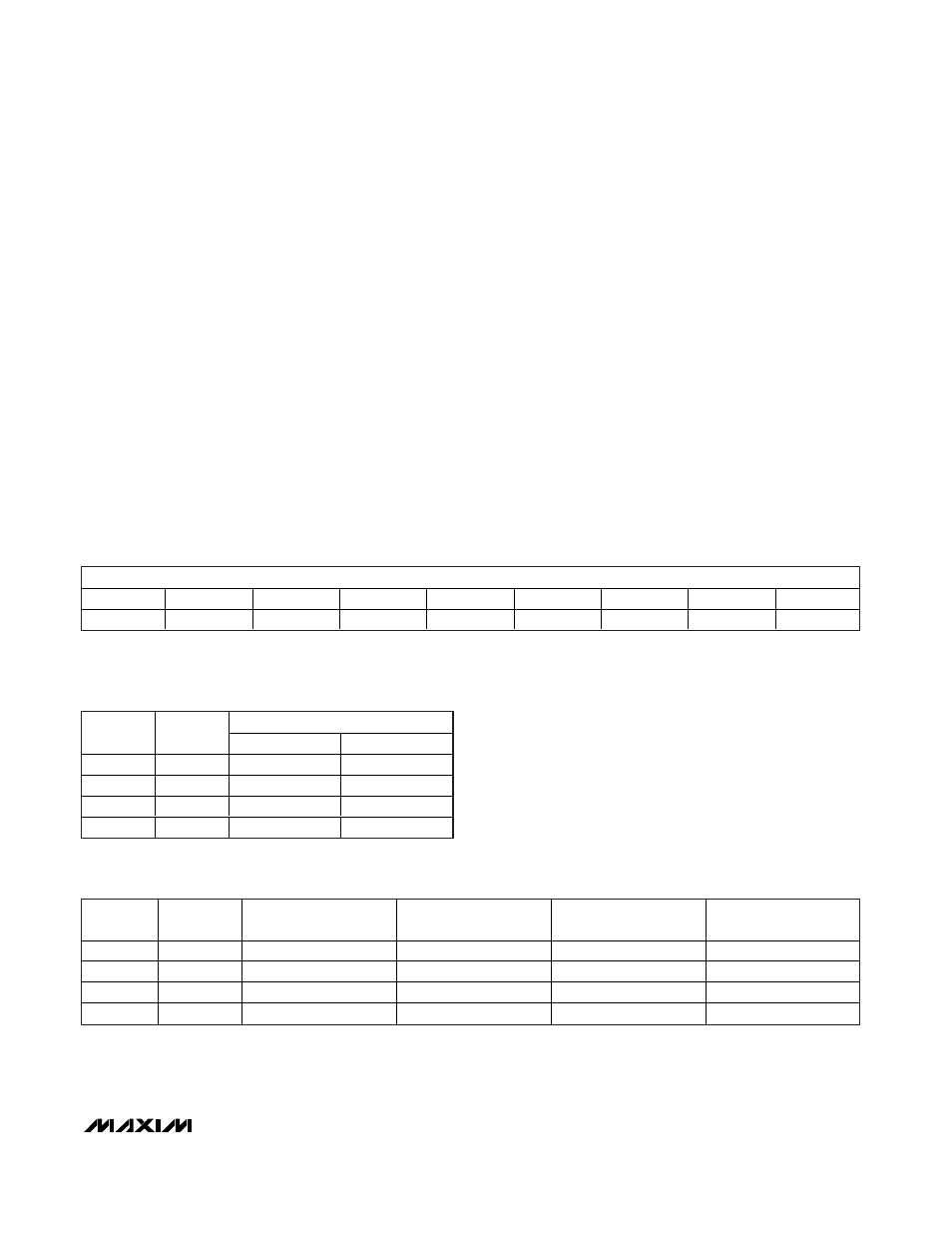
Table 20. ADC Acquisition Clock Bit
Configuration
ADC ACQUISITION CLOCKS
ACQCK1
ACQCK0
GAIN = 1, 2
GAIN = 4, 8
0
0
2
4
0
1
4
8
1
0
8
16
1
1
16
32
MSB
LSB
NAME
INTP
VM11
VM10
VM2CP2
VM2CP1
VM2CP0
CPDIV1
CPDIV0
DEFAULT
0
0
0
0
0
0
0
0