Synthesizing a sine wave – Rainbow Electronics MAX1329 User Manual
Page 70
MAX1329/MAX1330
12-/16-Bit DASs with ADC, DACs, DPIOs, APIOs,
Reference, Voltage Monitors, and Temp Sensor
70
______________________________________________________________________________________
Synthesizing a Sine Wave
The MAX1329/MAX1330 can easily create up to a
64-point single or periodic sine wave using the DACA
and FIFOA. The 16-word FIFO or memory is used to
create the first quarter of the waveform and symmetry is
used to extend the waveform to produce a complete
period. See the
DAC FIFO and Direct Digital Synthesis
(DDS) Logic
section for detailed waveform generation.
The first data point is the DACA input register data. The
FIFOA data is offset from this initial data. To determine
the values to be written to the FIFOA Data register use
the following equation.
FIFOA_DATA(n) = A x sin((n/N) x 90°)
where
n = 1 to N,
N = DPTA<3:0>,
A = (V
PEAK
/V
REFDAC
) x 4096,
V
PEAK
is the desired peak voltage of the sine wave,
and V
REFDAC
is the DAC reference voltage pro-
grammed at REFDAC.
Round the FIFOA_DATA(n) values to the nearest inte-
ger and write these values to the FIFOA Data register.
Figure 33 shows a sine wave with a 2V
P-P
output and
with a 1.25V offset. Write the DAC Control register with
0x43 to enable DACA, enable the internal reference,
and to set REFDAC to 2.5V. Write to the DACA input
and output register by performing a direct mode write
with 0x4800 to set DACA to midscale or 1.25V. Write
the FIFOA Control register with 0x7F to disable FIFOA
and allow a write to the FIFOA Data register, enabling
bipolar, symmetry, and continuous modes, and setting
the depth to 16.
The FIFOA data calculated from the above equation is
161, 320, 476, 627, 772, 910, 1039, 1159, 1267, 1362,
1445, 1514, 1568, 1607, 1631, and 1638 decimal. Write
the FIFOA Data register with 0x0A10 1400 1DC0 2730
3040 38E0 40F0 4870 4F30 5520 5A50 5EA0 6200
6470 65F0 6660 as a contiguous bit stream to fill the
FIFOA Data register with data. Write to the FIFOA
Control register with 0xFF to enable FIFOA and to disal-
low writes to the FIFOA Data register. Write to the DPIO
Control register with 0x0007 to program DPIO1 as an
input to sequence the DACA FIFO on each rising edge.
Write to the Switch Control register with 0x80 to close
the DACA switch to put the buffer into unity gain. Input
a continuous clock to DPIO1 that is 4 x N times (N = 16)
the desired frequency of the synthesized waveform.
Figure 33 should be observable on OUTA.
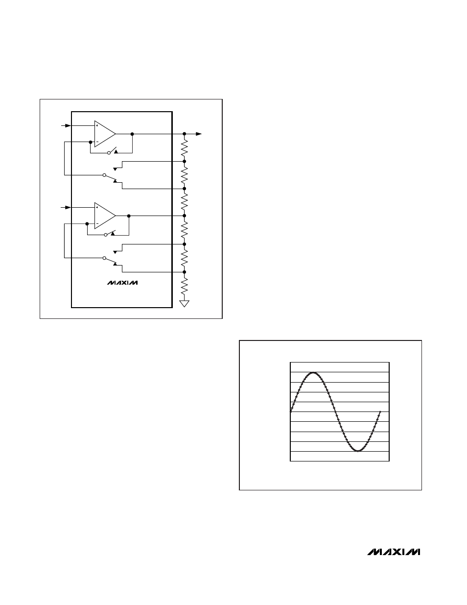
MAX1330
R
3
R
2
R
2
R
3
R
1
R
1
IN1+
IN1-
SCM1
V
OUT
SCM2
OUT1
SNO1
SNC1
SNO2
SNC2
V
IN+
V
IN-
OUT2
IN2+
IN2-
OA1
OSW1
SPDT1
OA2
OSW2
SPDT2
Figure 32. Programmable-Gain Instrumentation Amplifier,
Switch Position 1
0
0.75
0.50
0.25
1.25
1.00
2.25
2.00
1.75
1.50
2.50
0
10
20
30
40
50
60
70
SINE WAVE
DAC SEQUENCES
DAC OUTPUT (V)
Figure 33. Example Sine-Wave Output