Applications information, Power-supply considerations, Running directly off batteries – Rainbow Electronics MAX1329 User Manual
Page 63: Digital-interface connections
MAX1329/MAX1330
12-/16-Bit DASs with ADC, DACs, DPIOs, APIOs,
Reference, Voltage Monitors, and Temp Sensor
______________________________________________________________________________________
63
Applications Information
Power-Supply Considerations
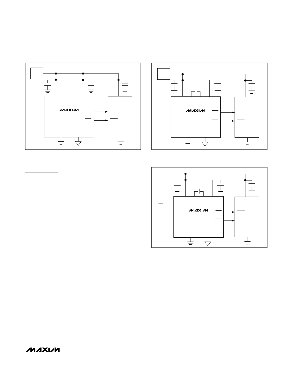
The circuit in Figure 23 applies an external 3.0V power
supply to both DV
DD
and AV
DD
. To drive AV
DD
directly,
disable the internal charge pump through the CP/VM
Control register. The bypass switch between DV
DD
and
AV
DD
can be either open or closed in this configuration.
Figure 24 shows the charge pump enabled to supply
AV
DD
. The charge-pump output voltage is set to 5.0V
through the CP/VM Control register. See the
Charge-
Pump Component Selection
section.
Figure 25 shows DV
DD
is powered from a battery with
the charge-pump output set to 3.0V. The charge pump
can draw high peak currents from DV
DD
under maxi-
mum load. Select an appropriately sized bypass capac-
itor for DV
DD
(≥ 10 times C
FLY
). Supply ripple can be
reduced by increasing CA
VDD
and/or the charge-pump
clock frequency.
Running Directly Off Batteries
The MAX1329/MAX1330 can be powered directly from
two alkaline cells, two silver oxide button cells, or a lithi-
um-coin cell. DV
DD
requires 1.8V to 3.6V and AV
DD
requires 2.7V to 5.5V for proper operation. Save power
by running DV
DD
directly off the battery and shorting to
AV
DD
by closing the internal bypass switch. Use the
2.7V AV
DD
voltage monitor to detect when it drops to
2.7V. Power is saved during this time because the inter-
nal charge pump is off. Once the battery voltage drops
to 2.7V, open the bypass switch and enable the internal
charge pump as long as DV
DD
is between 1.8V and
2.7V. Following this procedure optimizes the battery life.
Digital-Interface Connections
Figure 26 provides standard digital-interface connections
between the MAX1329/MAX1330 and a µC. The µC gen-
erates its own 32kHz clock for timekeeping and the
MAX1329/MAX1330 provide the high-frequency clock
required by the µC. See the
Clock Control Register
sec-
tion to program the CLKIO output and frequency and set
the ODLY bit to delay the turn-off time to enable the µC
time to go to sleep. During sleep, CLKIO becomes an
input and requires a weak pulldown resistor (≤1MΩ) to
minimize power dissipation. See the DPIO Setup and
DPIO Control registers to program DPIO1–DPIO4 as
wake-ups. Upon wake-up, the internal oscillator starts and
outputs to CLKIO. See the
CP/VM Control Register
sec-
tion to program the
RST1 and RST2 as a reset or interrupt.
MAX1329
MAX1330
DV
DD
C1A
C1B
AV
DD
DGND
AGND
INTERRUPT
V
DD
DGND
POWER
SUPPLY
0.1µF
0.1µF
0.1µF
2.7V TO 3.6V
µC
RST1
RST2
RESET
Figure 23. Power-Supply Circuit Using an External 3.0V Power
Supply for DV
DD
and AV
DD
MAX1329
MAX1330
DV
DD
RST1
C1A
C1B
AV
DD
DGND
AGND
INTERRUPT
V
DD
DGND
POWER
SUPPLY
0.1µF
2.7V TO 3.6V
C
FLY
5.0V
C
AVDD
C
DVDD
µC
RST2
RESET
Figure 24. Power-Supply Circuit Using an External 3.0V Power
Supply for DV
DD
and Internal Charge Pump Set to 5V for AV
DD
MAX1329
MAX1330
DV
DD
C1A
C1B
AV
DD
DGND
AGND
INTERRUPT
V
DD
DGND
0.1µF
1.8V TO 3.6V
C
FLY
3.0V
C
AVDD
C
DVDD
µC
E1
RST1
RST2
RESET
Figure 25. Power-Supply Circuit Using a Battery for DV
DD
and
Internal Charge Pump Set to 3.0V for AV
DD