Table 14. daca power-down bit configuration – Rainbow Electronics MAX1329 User Manual
Page 49
MAX1329/MAX1330
12-/16-Bit DASs with ADC, DACs, DPIOs, APIOs,
Reference, Voltage Monitors, and Temp Sensor
______________________________________________________________________________________
49
DAC Control Register
The DAC Control register configures the power states for
DACA, DACB, the op amps, DAC reference buffer, and
the internal reference. The DAC Control register also
controls the DACA and DACB input and output register
write modes. At power-up, all DACs and op amps are
powered down. When powered down, the outputs of the
DAC buffers and op amps are high impedance.
DAPD<1:0>: DACA Power-Down bits (default = 00).
DAPD<1:0> control the power-down states and write
modes for DACA (see Table 14).
DBPD<1:0>: (MAX1329 only) DACB Power-Down bits
(default = 00). DBPD<1:0> control the power-down states
and write modes for a DACB write as shown in Table 15.
OA1E: Op Amp 1 Enable bit (default = 0). Set OA1E = 1
to power up op amp 1.
OA2E (MAX1330 only): Op Amp 2 Enable bit (default =
0). Set OA2E = 1 to power up op amp 2.
DREF<1:0>: DAC Reference Buffer bits (default = 00).
DREF<1:0> sets the DAC reference buffer gain when
REFE = 0 (see Table 16). DREF<1:0> sets the REFDAC
voltage when the REFE = 1.
REFE: Internal Reference Enable bit (default = 0). REFE
= 1 enables the internal reference and sets REFADJ to
2.5V. REFE = 0 disables the internal reference so an
external reference can be applied at REFADJ, which
drives the inputs to the ADC and DAC reference
buffers. This bit is mirrored in the ADC Control register
so that writing either location updates both bits.
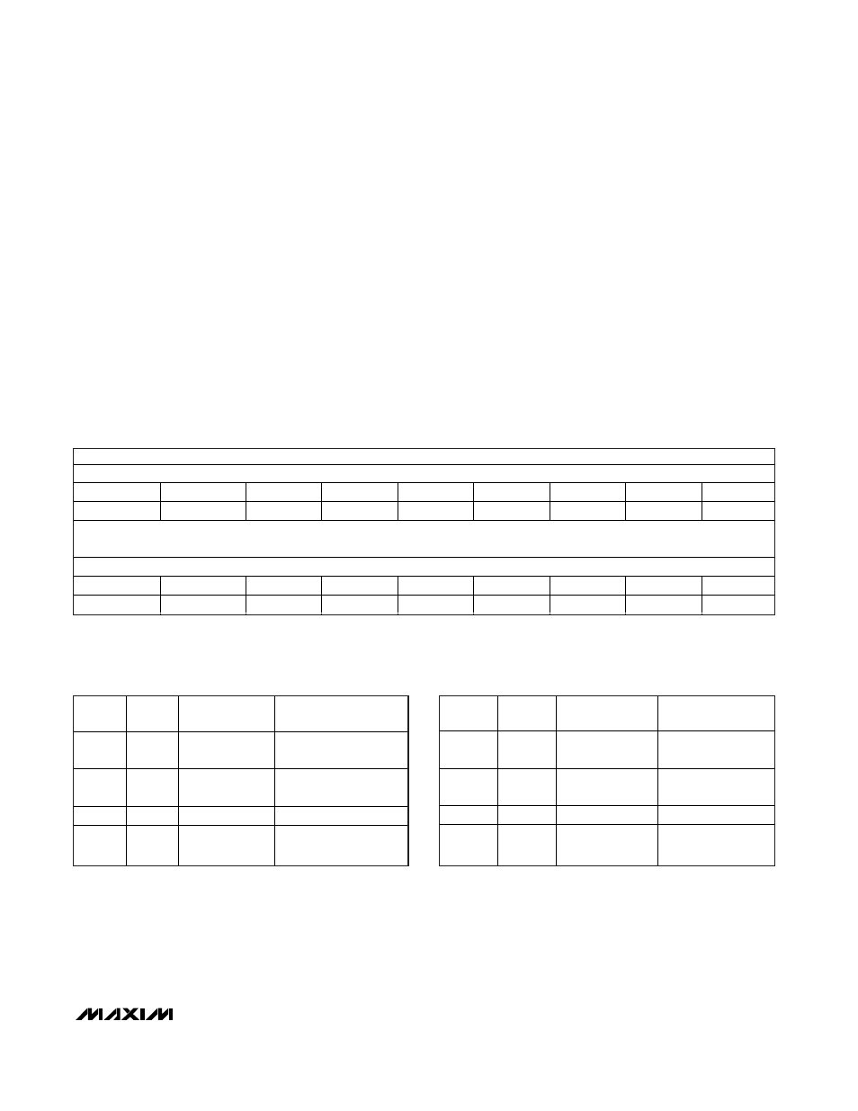
MAX1329
MSB
LSB
NAME
DAPD1
DAPD0
DBPD1
DBPD0
OA1E
DREF1
DREF0
REFE
DEFAULT
0
0
0
0
0
0
0
0
MAX1330
MSB
LSB
NAME
DAPD1
DAPD0
X
OA2E
OA1E
DREF1
DREF0
REFE
DEFAULT
0
0
X
0
0
0
0
0
Table 14. DACA Power-Down Bit
Configuration
DAPD1
DAPD0
DACA POWER
MODE
DACA WRITE MODE
0
0
Powered down
Write input and output
register
0
1
Powered up
Write input and output
register
1
0
Powered up
Write input register
1
1
Powered up
Shift input to output
register
Table 15. DACB Power-Down Bit
Configuration (MAX1329 Only)
DBPD1
DBPD0
DACB POWER
MODE
DACB WRITE
MODE
0
0
Powered down
Write input and
output register
0
1
Powered up
Write input and
output register
1
0
Powered up
Write input register
1
1
Powered up
Shift input to output
register