Rainbow Electronics MAX1329 User Manual
Page 42
MAX1329/MAX1330
12-/16-Bit DASs with ADC, DACs, DPIOs, APIOs,
Reference, Voltage Monitors, and Temp Sensor
42
______________________________________________________________________________________
ADC Setup Register
The ADC Setup register configures the input multiplexer,
ADC gain, and unipolar/bipolar modes to perform a data
conversion. Changes made to the ADC Setup register
settings are applied immediately. If changes are made
during a conversion in progress, discard the results of
that conversion to ensure a valid conversion result.
MSEL: Multiplexer Select bit (default = 0). The MSEL bit
selects the upper or lower multiplexer. MSEL = 0 selects
the upper mux and MSEL = 1 selects the lower mux.
MUX<3:0>: Multiplexer Input Select bits (default =
0000). The MUX<3:0> bits plus the MSEL bit select the
inputs to the ADC (see Tables 7 and 8).
GAIN<1:0>: ADC Gain bits (default = 00). The
GAIN<1:0> bits select the gain of the ADC (see Table 9).
BIP: Unipolar-/Bipolar-Mode Selection bit (default = 0).
For unipolar mode, set BIP = 0. For bipolar mode, set
BIP = 1. For temperature-sensor conversions, use the
default GAIN = 00 and BIP = 0.
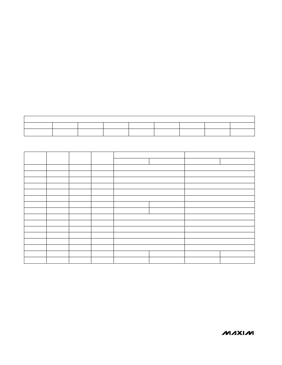
Table 7. Upper Multiplexer Bit Configuration (MSEL = 0)
POSITIVE INPUT
NEGATIVE INPUT
MUX3
MUX2
MUX1
MUX0
MAX1329
MAX1330
MAX1329
MAX1330
0
0
0
0
AIN1
AGND
0
0
0
1
AIN2
AGND
0
0
1
0
OUTA
AGND
0
0
1
1
FBA
AGND
0
1
0
0
OUT1
AGND
0
1
0
1
IN1-
AGND
0
1
1
0
OUTB
OUT2
AGND
0
1
1
1
FBB
IN2-
AGND
1
0
0
0
AIN1
AIN2
1
0
0
1
AIN2
AIN1
1
0
1
0
OUTA
FBA
1
0
1
1
FBA
OUTA
1
1
0
0
OUT1
IN1-
1
1
0
1
IN1-
OUT1
1
1
1
0
OUTB
OUT2
FBB
IN2-
1
1
1
1
FBB
IN2-
OUTB
OUT2
MSB
LSB
NAME
MSEL
MUX3
MUX2
MUX1
MUX0
GAIN1
GAIN0
BIP
DEFAULT
0
0
0
0
0
0
0
0