Rainbow Electronics MAX3541 User Manual
Page 2
MAX3541
Complete Single-Conversion
Television Tuner
2
_______________________________________________________________________________________
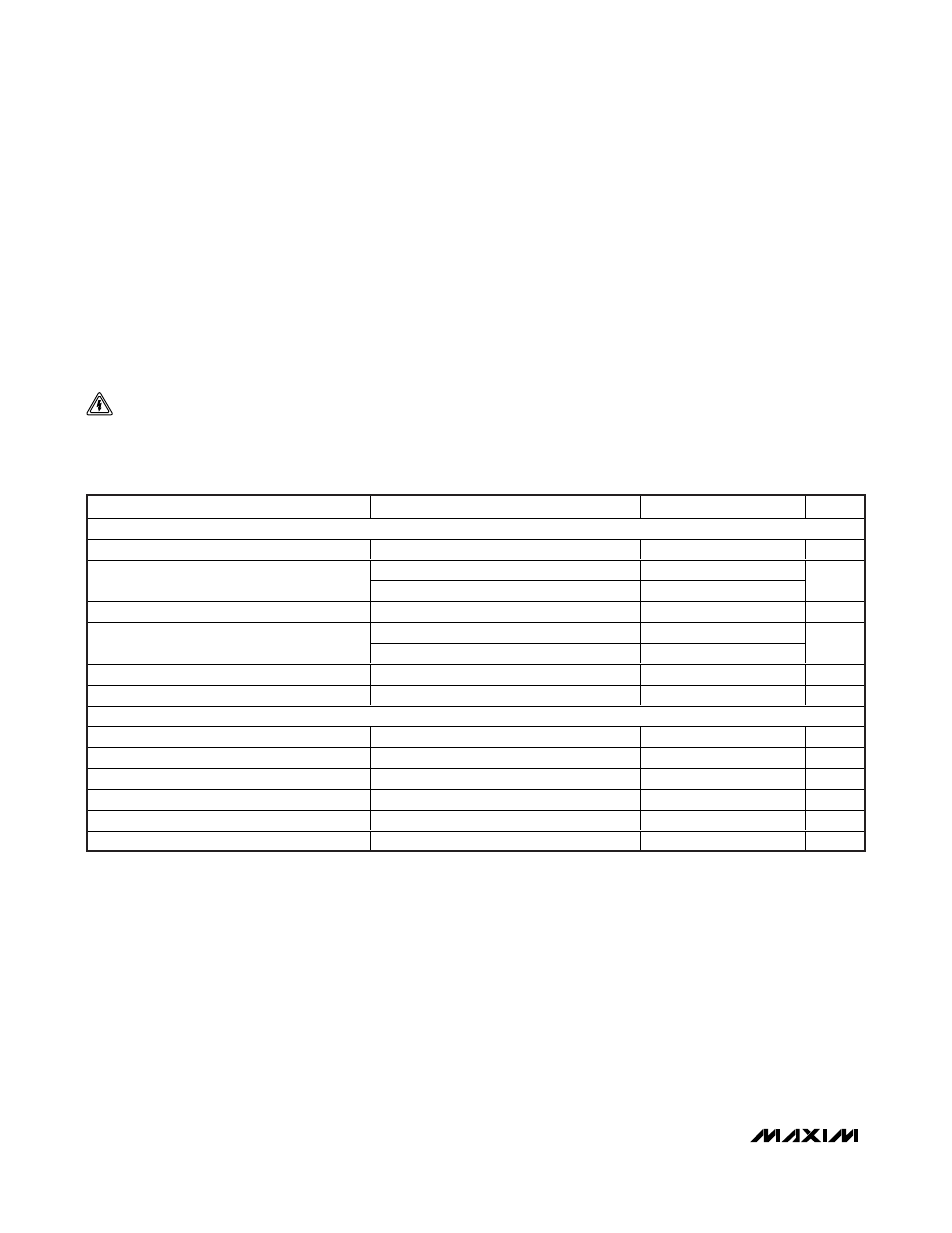
ABSOLUTE MAXIMUM RATINGS
DC ELECTRICAL CHARACTERISTICS
(MAX3541 EV kit, V
CC
= +3.1V to +3.5V, T
A
= -40°C to +85°C, no RF signals at RF inputs, default register settings, V
RFAGC
= V
IFAGC
= +3V (minimum attenuation), unless otherwise noted. Typical values are at V
CC
= +3.3V, T
A
= +25°C, unless otherwise noted.)
Stresses beyond those listed under “Absolute Maximum Ratings” may cause permanent damage to the device. These are stress ratings only, and functional
operation of the device at these or any other conditions beyond those indicated in the operational sections of the specifications is not implied. Exposure to
absolute maximum rating conditions for extended periods may affect device reliability.
V
CC
to GND ..............................................................-0.3V, +3.6V
RFIN, IFIN_ IFOUT1_, IFOUT2_, IFAGC, RFAGC,
VTUNE, LDO, MUX, CP,
XTAL to GND ....................................-0.3V to (V
CC
+ 0.3V)
SDA, SCL, ADDR2, ADDR1 to GND......................-0.3V to +3.6V
IFOUT__ Short-Circuit Duration .....................................Indefinite
RF Input Power ...............................................................+10dBm
Continuous Power Dissipation (T
A
= +70°C)
48-Pin fcLGA (derate 25mW/°C above +70°C) ..............1.4W
Operating Temperature Range ...........................-40°C to +85°C
Junction Temperature ......................................................+150°C
Storage Temperature Range .............................-65°C to +165°C
CAUTION! ESD SENSITIVE DEVICE
PARAMETER
CONDITIONS
MIN
TYP
MAX
UNITS
SUPPLY VOLTAGE AND CURRENT
Supply Voltage
+3.1
+3.5
V
Receive mode (SHDN = 3V)
230
275
Supply Current
Shutdown mode (SHDN = 0V)
5
mA
RF and IF AG C Inp ut Bi as C ur r ent
At +0.5V and +3V
-50
+50
μA
Minimum attenuation
+3
RF and IF AGC Control Voltage (Note 1)
Maximum attenuation
+0.5
V
Digital Input Logic-Level Low
0.3 x V
CC
V
Digital Input Logic-Level High
0.7 x V
CC
V
SERIAL INTERFACE
Input Logic-Level Low
0.3 x V
CC
V
Input Logic-Level High
0.7 x V
CC
V
Input Hysteresis
0.05 x V
CC
V
SDA, SCL Input Current
-10
+10
μA
Output Logic-Level Low
3mA sink current
0.4
V
Output Logic-Level High
V
CC
- 0.5
V