Rainbow Electronics MAX3541 User Manual
Page 13
MAX3541
Complete Single-Conversion
Television Tuner
______________________________________________________________________________________
13
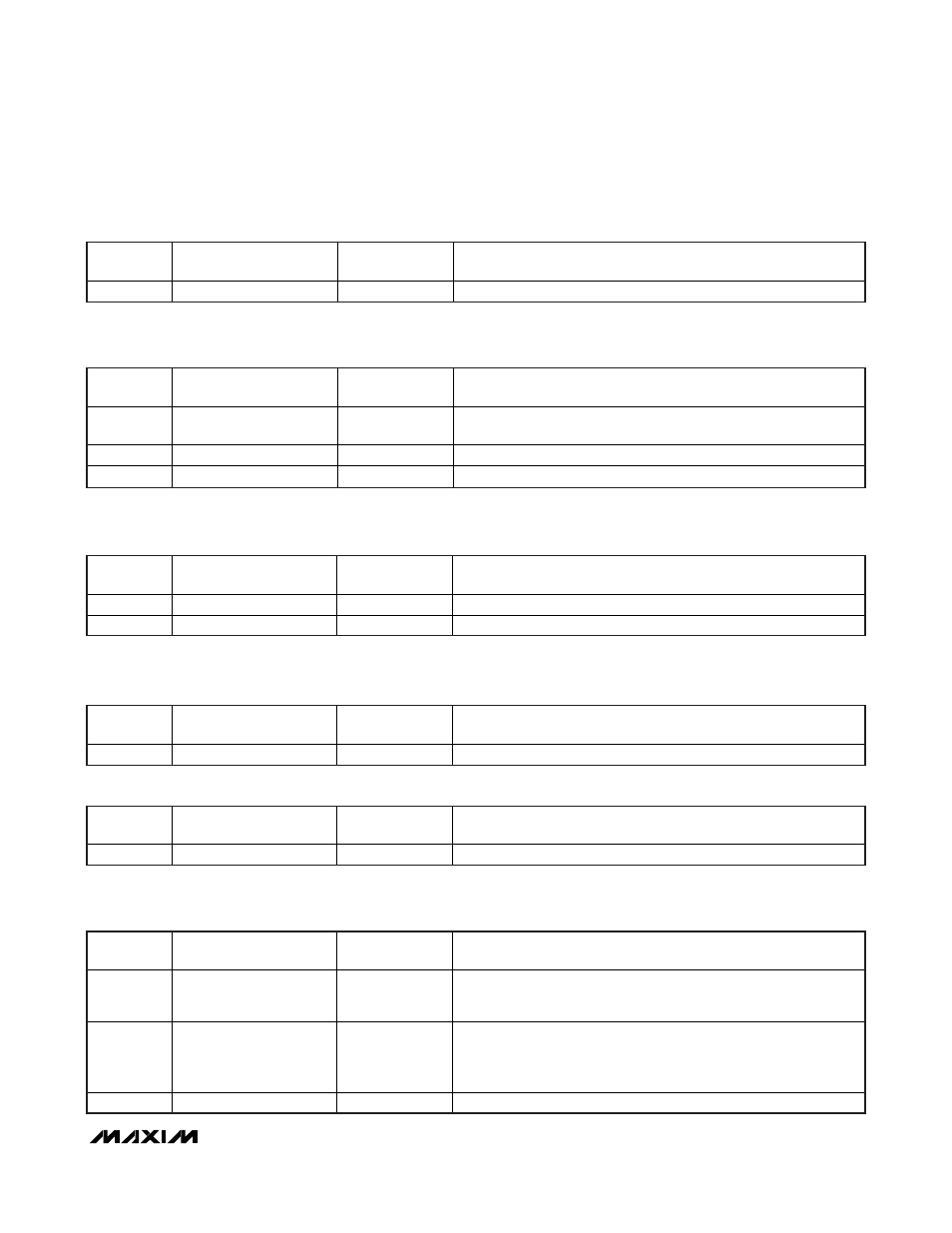
BIT NAME
BIT LOCATION (0 = LSB)
RECOMMENDED
DEFAULT
FUNCTION
TFS[7:0]
7-0
00001111*
Programs series capacitor values in the tracking filter.
Table 9. Tracking Filter Series Capacitor Register (Address: 0111
b
)
*See the
RF Tracking Filter
section.
BIT NAME
BIT LOCATION (0 = LSB)
RECOMMENDED
DEFAULT
FUNCTION
TFR[7:0]
7-0
00000000*
Tracking filter data bits read from the device’s ROM table.
Table 13. ROM Table Data Readback Register (Address: 1011
b
)
*See the
RF Tracking Filter
section.
BIT NAME
BIT LOCATION (0 = LSB)
RECOMMENDED
DEFAULT
FUNCTION
RESERVED
7-0
N/A
Reserved. Do not program these bits during normal operation.
Table 12. Reserved Register (Address: 1010
b
)
*See the
RF Tracking Filter
section.
*See the
RF Tracking Filter
section.
BIT NAME
BIT LOCATION (0 = LSB)
RECOMMENDED
DEFAULT
FUNCTION
FLD
7
0
Filter load bit. A 0 to 1 transition of this bit forces the loading of the
ROM Table Data Readback register.
RESERVED
6
0
Must be set to 0.
TFP[5:0]
5-0
001001*
Programs parallel capacitor values in the tracking filter.
Table 10. Tracking Filter Parallel Capacitor Register (Address: 1000
b
)
BIT NAME
BIT LOCATION (0 = LSB)
RECOMMENDED
DEFAULT
FUNCTION
RESERVED
7-4
0000
Must be set to 0000.
TFA[3:0]
3-0
0000*
Address bits of the ROM register to be read.
Table 11. Tracking Filter ROM Address Register (Address: 1001
b
)
BIT NAME
BIT LOCATION (0 = LSB)
RECOMMENDED
DEFAULT
FUNCTION
POR
7
N/A
Power-on reset.
0 = Status register has been read
1 = Power reset since last status register read
LD[2:0]
6-4
N/A
VCO tuning voltage indicators.
000 = PLL not in lock, tune to the next lowest sub-band
001–110 = PLL in lock
111 = PLL not in lock, tune to the next higher sub-band
RESERVED
3-0
N/A
Reserved.
Table 14. Status Register (Address: 1100
b
)