Chip information – Rainbow Electronics MAX1479 User Manual
Page 8
MAX1479
300MHz to 450MHz Low-Power,
Crystal-Based +10dBm ASK/FSK Transmitter
8
_______________________________________________________________________________________
Output Matching to
PC Board Loop Antenna
In most applications, the MAX1479 power-amplifier out-
put has to be impedance matched to a small-loop
antenna. The antenna is usually fabricated out of a cop-
per trace on a PC board in a rectangular, circular, or
square pattern. The antenna has an impedance that
consists of a lossy component and a radiative compo-
nent. To achieve high radiating efficiency, the radiative
component should be as high as possible, while mini-
mizing the lossy component. In addition, the loop
antenna has an inherent loop inductance associated
with it (assuming the antenna is terminated to ground).
For example, in a typical application, the radiative
impedance is less than 0.5
Ω, the lossy impedance is
less than 0.7
Ω, and the inductance is approximately
50nH to 100nH.
The objective of the matching network is to match the
power-amplifier output to the impedance of the small-
loop antenna. The matching components thus tune out
the loop inductance and transform the low radiative
and resistive parts of the antenna into the much higher
value of the PA output. This gives higher efficiency. The
low radiative and lossy components of the small-loop
antenna result in a higher Q matching network than the
50
Ω network; thus, the harmonics are lower.
Layout Considerations
A properly designed PC board is an essential part of
any RF/microwave circuit. On the power-amplifier out-
put, use controlled-impedance lines and keep them as
short as possible to minimize losses and radiation.
Keeping the traces short reduces parasitic inductance.
Generally, 1in of PC board trace adds about 20nH of
parasitic inductance. Parasitic inductance can have a
dramatic effect on the effective inductance. For exam-
ple, a 0.5in trace connecting a 100nH inductor adds an
extra 10nH of inductance, or 10%.
To reduce the parasitic inductance, use wider traces
and a solid ground or power plane below the signal
traces. Using a solid ground plane can reduce the par-
asitic inductance from approximately 20nH/in to 7nH/in.
Also, use low-inductance connections to ground on all
GND pins and place decoupling capacitors close to all
V
DD
connections.
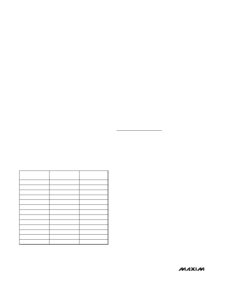
Chip Information
TRANSISTOR COUNT: 2369
PROCESS: CMOS
COMPONENT
VALUE FOR
f
RF
= 433MHz
VALUE FOR
f
RF
= 315MHz
L1
22nH
27nH
L3
18nH
22nH
C1
6.8pF
15pF
C2
10pF
22pF
C3
10nF
10nF
C4
680pF
680pF
C6
6.8pF
15pF
C8
220pF
220pF
C10
10nF
10nF
C11
220pF
220pF
C12
220pF
220pF
C14
100pF
100pF
C15
100pF
100pF
Table 3. Component Values for Typical
Application Circuit