Applications information, Table 1. clock divider settings, Table 2. frequency-deviation settings – Rainbow Electronics MAX1479 User Manual
Page 7
MAX1479
300MHz to 450MHz Low-Power,
Crystal-Based +10dBm ASK/FSK Transmitter
_______________________________________________________________________________________
7
Clock Output
The MAX1479 has a dedicated digital output pin for the
frequency-divided crystal clock signal. This is to be
used as the time base for a microprocessor. The fre-
quency-division ratio is programmable through two dig-
ital input pins (CLK0, CLK1), and is defined in Table 1.
The clock output is designed to drive a 3.5MHz CMOS
rail-to-rail signal into a 10pF capacitive load.
Envelope-Shaping Resistor
The envelope-shaping resistor allows for a gentle turn-
on/turn-off of the PA in ASK mode. This results in a small-
er spectral width of the modulated PA output signal.
Phase-Locked Loop
The PLL block contains a phase detector, charge
pump, integrated loop filter, VCO, asynchronous 32x
clock divider, and crystal oscillator. The PLL requires
no external components. The relationship between the
carrier and crystal frequency is given by:
f
XTAL
= f
RF
/ 32
Crystal Oscillator
The crystal oscillator in the MAX1479 is designed to
present a capacitance of approximately 3pF to ground
from the XTAL1 and XTAL2 pins in ASK mode. In most
cases, this corresponds to a 4.5pF load capacitance
applied to the external crystal when typical PC board
parasitics are added. In FSK mode, a percentage
(defined by bits DEV0 to DEV2) of the 3pF internal crys-
tal oscillator capacitance is removed for a logic 1 on
the DIN pin to pull the transmit frequency. The frequen-
cy deviation is shown in Table 2. It is very important
to use a crystal with a load capacitance that is equal
to the capacitance of the MAX1479 crystal oscillator
plus PC board parasitics. If very large FSK frequency
deviations are desired, use a crystal with a larger
motional capacitance and/or reduce PC board parasitic
capacitances.
Power Amplifier
The PA of the MAX1479 is a high-efficiency, open-drain,
class-C amplifier. With a proper output-matching net-
work, the PA can drive a wide range of impedances,
including small-loop PC board trace antennas and any
50
Ω antennas. The output-matching network for a 50Ω
antenna is shown in the Typical Application Circuit. The
output-matching network suppresses the carrier harmon-
ics and transforms the antenna impedance to an optimal
impedance at PAOUT (pin 8), which is about 250
Ω.
When the output-matching network is properly tuned,
the power amplifier is highly efficient. The Typical
Application Circuit delivers +10dBm at a supply volt-
age of +2.7V, and draws a supply current of 6.7mA for
ASK/OOK operation (V
DIN
at 50% duty cycle) and
10.5mA for FSK operation. Thus, the overall efficiency
at 100% duty cycle is 35%. The efficiency of the power
amplifier itself is about 50%. An external resistor at
ROUT sets the output power.
Applications Information
Output Matching to 50
Ω
When matched to a 50
Ω system, the MAX1479 PA is
capable of delivering more than +10dBm of output
power at V
DD
= 2.7V. The output of the PA is an open-
drain transistor that requires external impedance
matching and pullup inductance for proper biasing.
The pullup inductance from PAOUT to V
DD
serves three
main purposes: It forms a resonant tank circuit with the
capacitance of the PA output, provides biasing for the
PA, and becomes a high-frequency choke to reduce
the RF energy coupling into V
DD
. Maximum efficiency is
achieved when the PA drives a load of 250
Ω. The rec-
ommended output-matching network topology is shown
in the Typical Application Circuit.
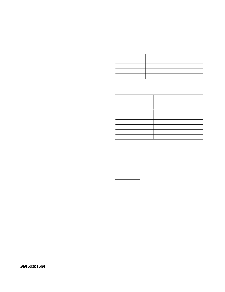
CLK1
CLK0
CLKOUT
0
0
Logic 0
0
1
f
XTAL
/ 4
1
0
f
XTAL
/ 8
1
1
f
XTAL
/ 16
Table 1. Clock Divider Settings
DEV2
DEV1
DEV0
DEVIATION
0
0
0
1/8 x max
0
0
1
1/4 x max
0
1
0
3/8 x max
0
1
1
1/2 x max
1
0
0
5/8 x max
1
0
1
3/4 x max
1
1
0
7/8 x max
1
1
1
Max
Table 2. Frequency-Deviation Settings