Rainbow Electronics MAX1479 User Manual
Page 2
MAX1479
300MHz to 450MHz Low-Power,
Crystal-Based +10dBm ASK/FSK Transmitter
2
_______________________________________________________________________________________
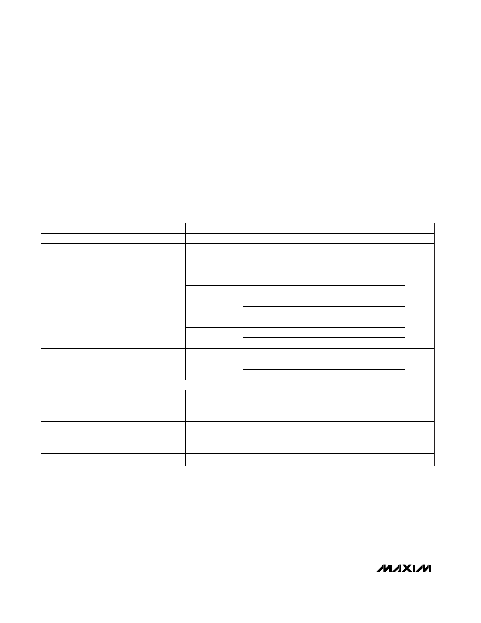
ABSOLUTE MAXIMUM RATINGS
DC ELECTRICAL CHARACTERISTICS
(Typical Application Circuit, all RF inputs and outputs are referenced to 50
Ω, V
DD
= +2.1V to +3.6V, V
ENABLE
= V
DD
, T
A
= -40°C to
+125°C, unless otherwise noted. Typical values are at V
DD
= +2.7V, T
A
= +25°C, unless otherwise noted.) (Note 1)
Stresses beyond those listed under “Absolute Maximum Ratings” may cause permanent damage to the device. These are stress ratings only, and functional
operation of the device at these or any other conditions beyond those indicated in the operational sections of the specifications is not implied. Exposure to
absolute maximum rating conditions for extended periods may affect device reliability.
V
DD
to GND .............................................................-0.3V to +4V
All Other Pins to GND ................................-0.3V to (V
DD
+ 0.3V)
Continuous Power Dissipation (T
A
= +70°C)
16-Pin Thin QFN (derate 14.7mW/°C above +70°C)...1176.5mW
Operating Temperature Range .........................-40°C to +125°C
Junction Temperature ......................................................+150°C
Storage Temperature Range .............................-60°C to +150°C
Lead Temperature (soldering, 10s) .................................+300°C
PARAMETER
SYMBOL
CONDITIONS
MIN
TYP
MAX
UNITS
Supply Voltage
V
DD
2.1
3.6
V
f
RF
= 315MHz
2.9
4.3
PA off, V
DIN
at
0% duty cycle
(ASK or FSK)
(Note 2)
f
RF
= 433MHz
3.3
4.8
f
RF
= 315MHz
6.7
10.7
V
DIN
at 50% duty
cycle (ASK)
(Notes 3, 4)
f
RF
= 433MHz
7.3
11.4
f
RF
= 315MHz (Note 2)
10.5
17.1
Supply Current
I
DD
V
DIN
at 100%
duty cycle (FSK)
f
RF
= 433MHz (Note 4)
11.4
18.1
mA
T
A
= +25°C
0.2
T
A
< +85
°C (Note 4)
120
300
Standby Current
I
STDBY
V
ENABLE
< V
IL
T
A
< +125
°C (Note 2)
700
1600
nA
DIGITAL INPUTS AND OUTPUTS
Data Input High
V
IH
(Note 2)
V
DD
-
0.25
V
Data Input Low
V
IL
(Note 2)
0.25
V
Maximum Input Current
I
IN
20
µA
Output Voltage High
V
OH
CLKOUT, load = 10k
Ω || 10pF (Note 4)
V
DD
-
0.25
V
Output Voltage Low
V
OL
CLKOUT, load = 10k
Ω || 10pF (Note 4)
0.25
V