Ac electrical characteristics – Rainbow Electronics MAX1479 User Manual
Page 3
MAX1479
300MHz to 450MHz Low-Power,
Crystal-Based +10dBm ASK/FSK Transmitter
_______________________________________________________________________________________
3
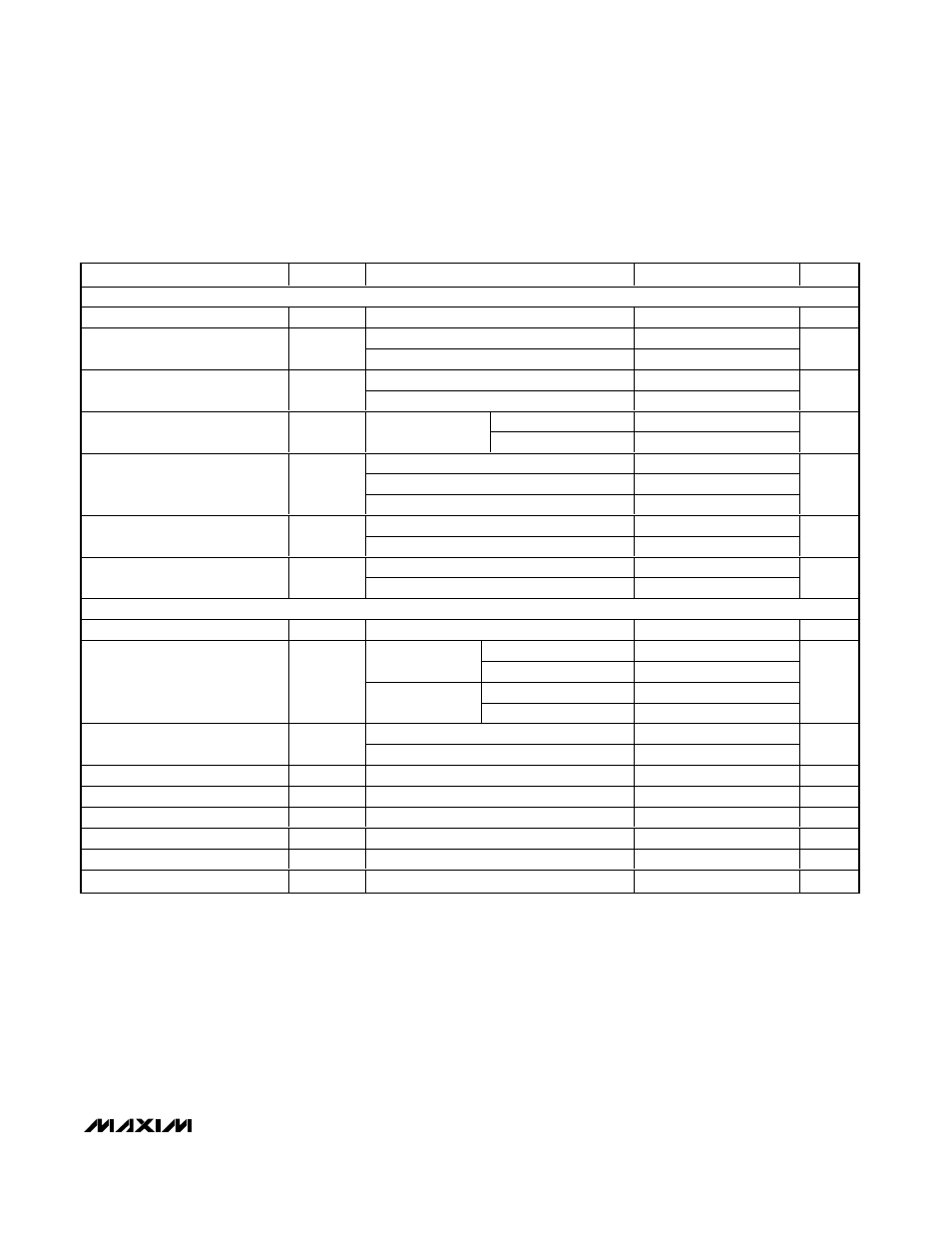
Note 1: Supply current, output power, and efficiency are greatly dependent on board layout and PAOUT match.
Note 2: 100% tested at T
A
= +125°C. Guaranteed by design and characterization over temperature.
Note 3: 50% duty cycle at 10kHz ASK data (Manchester coded).
Note 4: Guaranteed by design and characterization, not production tested.
Note 5: V
ENABLE
= V
IL
to V
ENABLE
= V
IH
. f
OFFSET
is defined as the frequency deviation from the desired carrier frequency.
Note 6: Dependent on crystal and PC board trace capacitance.
Note 7: V
ENABLE
> V
IH
, V
DATA
> V
IH
, Efficiency = P
OUT
/ (V
DD
x I
DD
).
Note 8: Dependent on PC board trace capacitance.
PARAMETER
SYMBOL
CONDITIONS
MIN
TYP
MAX
UNITS
SYSTEM PERFORMANCE
Frequency Range
f
RF
(Note 2)
300
450
MHz
Settle to within 50kHz
200
Turn-On Time (Note 5)
t
ON
Settle to within 5kHz
350
µs
ASK mode (Manchester coded)
100
Maximum Data Rate (Note 4)
FSK mode (Manchester coded)
20
kbps
f
RF
= 315MHz
55
Maximum FSK Frequency
Deviation
DEV[2:0] = 111
(Note 6)
f
RF
= 433MHz
80
kHz
T
A
= +25°C, V
DD
= +2.7V
6.8
10
12.0
T
A
= +125°C, V
DD
= +2.1V
2.7
5.3
Output Power (Note 2)
P
OUT
T
A
= -40°C, V
DD
= +3.6V
12.2
16.1
dBm
f
RF
= 315MHz
35
Transmit Efficiency with CW Tone
(Note 7)
f
RF
= 433MHz
34
%
f
RF
= 315MHz
27
Transmit Efficiency at 50% Duty
Cycle
f
RF
= 433MHz
25
%
PHASE-LOCKED-LOOP PERFORMANCE
VCO Gain
K
VCO
280
MHz/V
f
OFFSET
= 100kHz
-75
f
RF
= 315MHz
f
OFFSET
= 1MHz
-98
f
OFFSET
= 100kHz
-74
Phase Noise
f
RF
= 433MHz
f
OFFSET
= 1MHz
-98
dBc/Hz
f
RF
= 315MHz
-50
Maximum Carrier Harmonics
f
RF
= 433MHz
-45
dBc
Reference Spur
-40
dBc
Loop Bandwidth
BW
300
kHz
Crystal Frequency Range
f
XTAL
f
RF
/32
MHz
Crystal Tolerance
50
ppm
Crystal Load Capacitance
C
LOAD
(Note 8)
4.5
pF
Clock Output Frequency
D eter m i ned b y C LK0 and C LK1; see Tab l e 1
F
XTAL
/ N
MHz
AC ELECTRICAL CHARACTERISTICS
(Typical Application Circuit, all RF inputs and outputs are referenced to 50
Ω, V
DD
= +2.1V to +3.6V, V
ENABLE
= V
DD
, T
A
= -40°C to
+125°C, unless otherwise noted. Typical values are at V
DD
= +2.7V, T
A
= +25°C, unless otherwise noted.) (Note 1)