Max3941, 10gbps eam driver with integrated bias network, Detailed description – Rainbow Electronics MAX3941 User Manual
Page 8: Pin description
MAX3941
Detailed Description
The MAX3941 EAM driver consists of two main parts: a
high-speed modulation driver and an EAM-biasing
block. The clock and data inputs to the driver are com-
patible with PECL and CML logic levels. The modula-
tion and bias currents are output through the OUT pin.
The modulation output stage is composed of a high-
speed differential pair and a programmable current
source with a maximum modulation current of 120mA.
The rise and fall times are typically 23ps. The modulation
current is designed to produce an EAM voltage up to
3.0V
P-P
when driving a 50
Ω module. The 3.0V
P-P
results
from 120mA
P-P
through the parallel combination of the
50
Ω EAM load and the internal 50Ω back termination.
Polarity Switch
The MAX3941 includes a polarity switch. When the
PLRT pin is high or left floating, the output maintains the
polarity of the input data. When the PLRT pin is low, the
output is inverted relative to the input data.
Clock/Data Input Logic Levels
The MAX3941 is directly compatible with ground-refer-
ence CML. Either DC- or AC-coupling can be used for
CML referenced to ground. For all other logic types,
AC-coupling should be used.
Optional Data Input Latch
To reject pattern-dependent jitter in the input data, a syn-
chronous differential clock signal should be connected to
the CLK+ and CLK- inputs, and the RTEN control input
should be connected to V
EE
.
10Gbps EAM Driver with Integrated
Bias Network
8
_______________________________________________________________________________________
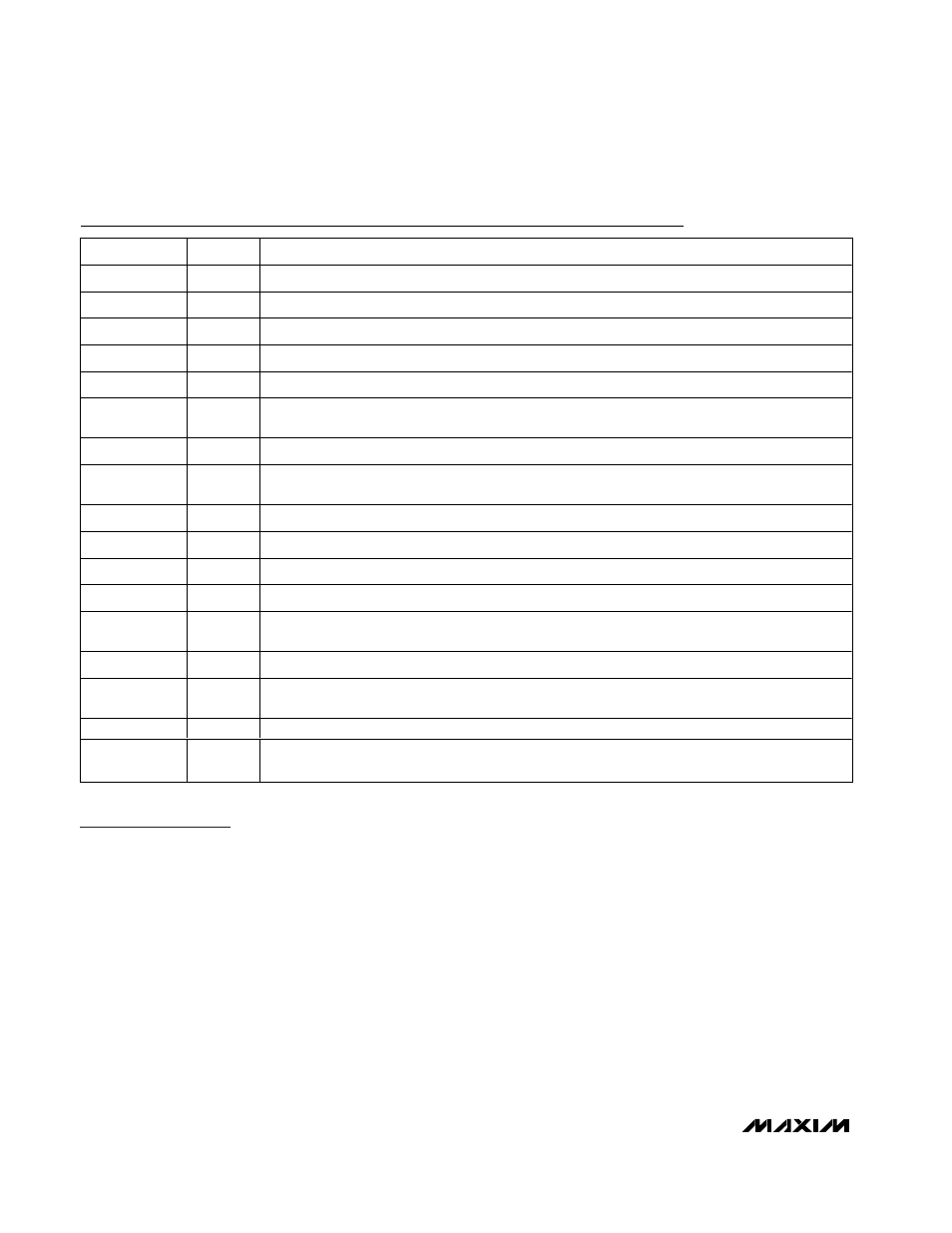
PIN
NAME
FUNCTION
1
DATA+
Noninverting Data Input with 50
Ω On-Chip Termination
2
DATA-
Inverting Data Input with 50
Ω On-Chip Termination
3, 4, 14
GND
Ground. All pins must be connected to board ground.
5
CLK+
Noninverting Clock Input for Data Retiming with 50
Ω On-Chip Termination
6
CLK-
Inverting Clock Input for Data Retiming with 50
Ω On-Chip Termination
7, 11, 12, 13,
18, 19, 24
V
EE
Negative Supply Voltage. All pins must be connected to board V
EE
.
8
PWC+
Positive Input for Modulation Pulse-Width Adjustment (See the Design Procedure Section)
9
PWC-
Negative Input for Modulation Pulse-Width Adjustment. Ground to disable the pulse-width
adjustment feature (see the Design Procedure section).
10
MODSET
Modulation Current Set. Apply a voltage to set the modulation current of the driver output.
15
GND1
Ground. Ground connection.
16
OUT
Driver Output. Provides both modulation and bias output. DC-couple to EAM.
17
GND2
Ground. Ground connection.
20
PLRT
Differential Data Polarity Swap Input. Set high or float for normal operation. Set low to invert the
differential signal polarity. Contains an internal 100k
Ω pullup to GND.
21
BIASSET
Bias Current Set. Apply a voltage to set the bias current of the driver output.
22
MODEN
TTL/CMOS Modulation Enable Input. Set low or float for normal operation. Set high to put the EAM
in the absorption (logic 0) state. Contains an internal 100k
Ω pulldown to V
EE
.
23
RTEN
Data-Retiming Input. Connect to V
EE
for retimed data. Connect to GND to bypass retiming latch.
EP
Exposed
Pad
Ground. Must be soldered to the circuit board ground for proper thermal and electrical performance
(see the Exposed Pad Package section).
Pin Description