Ds1843 fast sample-and-hold circuit, Applications information – Rainbow Electronics DS1843 User Manual
Page 7

DS1843
Fast Sample-and-Hold Circuit
_______________________________________________________________________________________
7
Applications Information
Power-Supply Decoupling
To achieve the best results when using the DS1843,
decouple the power-supply pin, V
CC
, with a 0.01μF or
0.1μF capacitor. Use a high-quality X7R or equivalent
ceramic surface-mount capacitor.
DS1843 Estimated Settling Time
The settling time is dependent on the gain ratio of the
current mirror used at the input of the DS1843. For
example, the MAX4007 includes a 10:1 ratio current
mirror. This requires a 5k
Ω resistor to create a 1V full-
scale output with 2mA current input to the MAX4007.
This resistor can be decreased to 2.5k
Ω by using the
DS1842, which has a 5:1 ratio current mirror.
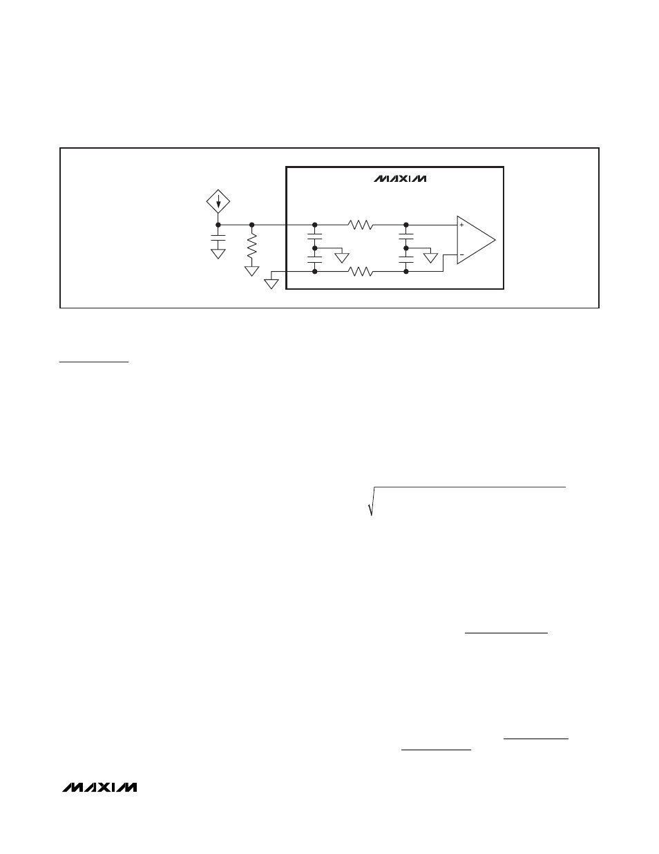
Variable Definitions:
R
IN
: Input resistor. The current mirror creates a voltage
across this resistor.
R
SW
: Resistance of series switch that connects internal
circuitry to input pins after t
IST
time.
C
IN
: 7pF parasitic (ESD) capacitor.
C
PAR
: External parasitic capacitance. A current mirror's
output and typical trace capacitance are less than
10pF.
C
S
: 5pF sample capacitor.
t
IST
: Internal settling time based on t
S
from the AC elec-
trical specification. The minimum t
S
includes one time
constant. t
IST
removes this time constant.
t
RC
: RC settling time of the input.
Figure 1 shows the simplified diagram of input imped-
ances for settling time calculations. Sample time is
divided into two parts:
1) t
IST
: Internal settling time (max 250ns). During this
time, voltage V
IN
(V
INP
- V
INN
) rises with a time con-
stant of:
R
IN
x (C
IN
+ C
PAR
)
2) t
RC
: During this period two things happen:
a. Input V
IN
keeps increasing from its value at t
IST
to its final value with a new time constant of:
b. R
SW
and C
S
track this V
IN
(input) with a time con-
stant of R
SW
x C
S
, which is 12.5ns (worst case).
Example:
Approximate accuracy calculations can be done for an
input voltage based on the above impedance values.
These calculations can be divided into three parts.
1) Accuracy of input at t
IST
(250ns):
where t
1
= t
IST
= 250ns.
At t
IST
the internal circuit tags input impedance.
This causes charge redistribution to occur, which
causes a dip in the input voltage. The worst-case
value of the input voltage at t
IST
is:
V
C
C
C
C
e
IN
t
S
IN
PAR
S
t
IST
IST
@
=
−
+
+
(
)
⎡
⎣
⎢
⎢
⎤
⎦
⎥
⎥
× −
−
1
1
R
R
C
C
IN
IN
IN
PAR
V
Ч
+
(
)
⎡⎣
⎤⎦
⎡
⎣
⎢
⎢
⎢
⎢
⎤
⎦
⎥
⎥
⎥
⎥
Ч
Accuracy
e
t
R
C
C
IN
IN
PAR
= −
−
×
+
(
)
⎡⎣
⎤⎦
1
1
R
C
C
R
C
IN
IN
PAR
SW
S
Ч
+
(
)
(
)
+
Ч
(
)
⎧
⎨
⎩
⎫
⎬
⎭
2
2
DS1843
C
S
C
S
C
IN
C
PAR
C
IN
INPUT MODEL
R
SW
V
INP
V
INN
R
SW
R
IN
CURRENT
MIRROR OUTPUT
Figure 1. Input Impedances for Settling Time Calculations Diagram
