Ds1843 fast sample-and-hold circuit, Detailed description, Pin description – Rainbow Electronics DS1843 User Manual
Page 6: Block diagram

DS1843
Fast Sample-and-Hold Circuit
6
_______________________________________________________________________________________
Detailed Description
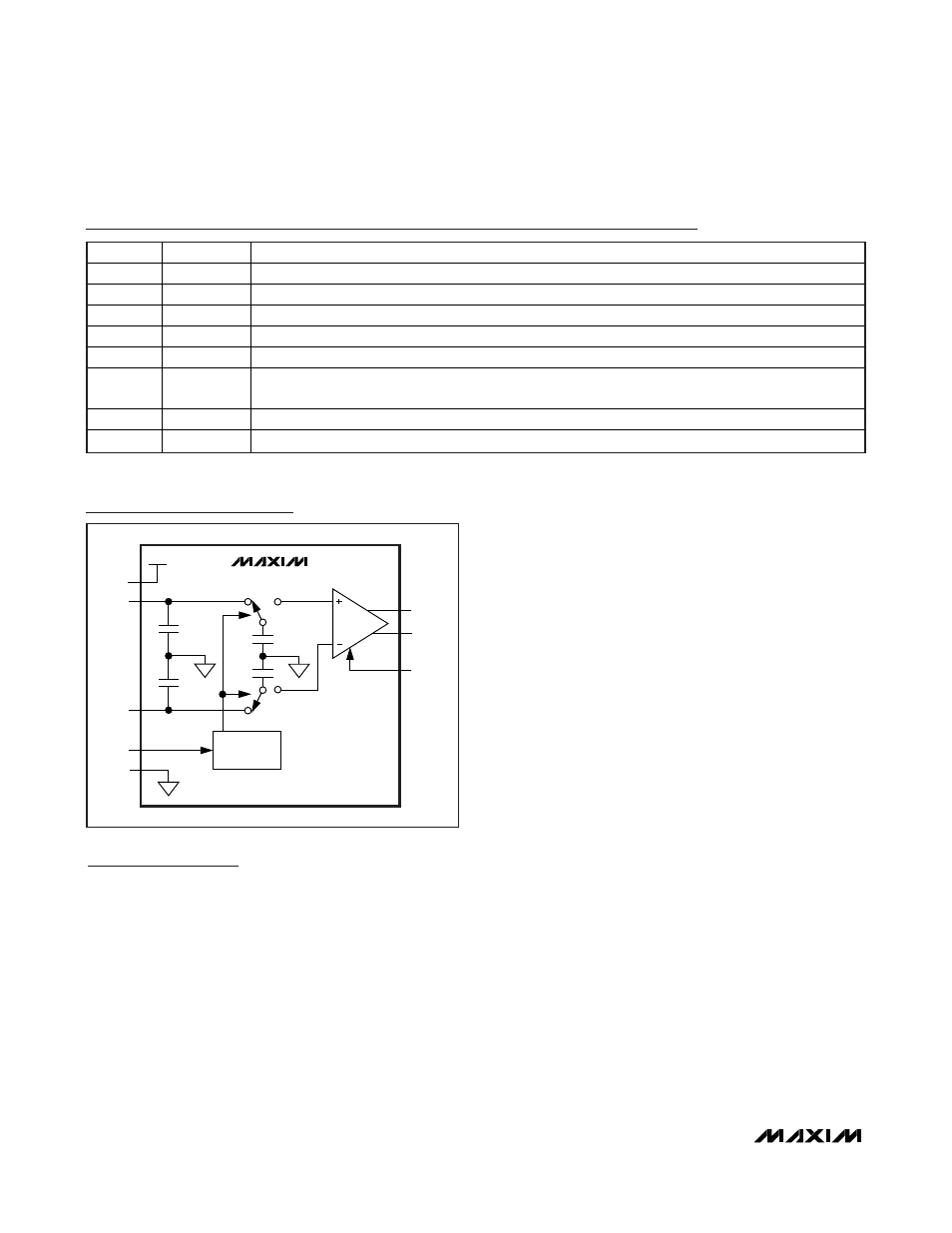
The DS1843 consists of a fully differential sampling
capacitor, switches, and a differential output buffer. It is
designed to operate in fiber optic burst-mode systems;
however, it can be used in other applications requiring
a fast sample-and-hold circuit. The output can be con-
figured for single-ended operations.
Input Sampling Capacitor
The input voltage is sampled using a 5pF capacitor on
the positive input and another on the negative input.
The capacitors are connected to the input when SEN is
high. In addition to the sampling capacitors, the inputs
also have parasitic capacitance (C
IN
). These capaci-
tors must fully charge before SEN is switched to low in
order to ensure accurate sampling. An RC time con-
stant is created by the resistance of the voltage source
connected to the DS1843’s input and the capacitances
on this node. See the
Applications Information
section
for details.
Output Buffer
After sampling is complete, the sampling capacitor is
switched to the output buffer. This buffer requires a
small amount of time to settle, t
OUT
. When an ADC is
used to measure the DS1843’s output, a step occurs at
the ADC’s input caused by the ADC’s internal sampling
capacitor. The DS1843’s recovery time, t
REC
, is depen-
dent on the size of the ADC’s sampling capacitor and
the voltage applied across the ADC. To maximize
accuracy, the ADC’s sampling speed (ADC clock fre-
quency) should be reduced until the ADC’s conversion
window (t
ADC:ST
, as shown in the
Timing Diagram
) is
larger than the DS1843’s recovery time. Refer to the
ADC’s documentation for t
ADC:ST
.
Sampling Time and Output Error
As the sampling time (t
S
) is decreased, the output error
increases. The output error is largely dependent on the
settling time of the sampling capacitor and, to a lesser
degree, the output buffer’s gain error and offset volt-
age. Settling time can be reduced by driving the
DS1843 with a lower impedance. In a typical fiber optic
application, a current is applied across a 5k
Ω resistor.
By using a stronger current source, the resistance and
the settling time can be reduced (see the
Applications
Information
section for details).
Pin Description
PIN
NAME
FUNCTION
1 V
CC
Power-Supply
Input
2 V
INP
Positive Voltage Input. Input to sample circuit.
3 V
INN
Negative Voltage Input. Input to sample circuit.
4
DEN
Differential Output Enable. Connect to V
CC
for differential output or GND for single-ended output.
5 GND
Ground
Terminal
6 V
OUTN
Sampled Voltage Negative Output. Buffered output of the hold capacitor. Keep unconnected or
connect to GND for single-ended output mode.
7 V
OUTP
Sampled Voltage Positive Output and Single-Ended Output. Buffered output of the hold capacitor.
8
SEN
Sample Enable. Enables input sampling. This input is pulsed.
Block Diagram
DS1843
V
OUTN
C
S
C
S
V
CC
V
INP
V
INN
SEN
GND
C
IN
C
IN
V
OUTP
CONTROL
LOGIC
DEN
