Ds1843 fast sample-and-hold circuit, Timing diagram, Ac electrical characteristics – Rainbow Electronics DS1843 User Manual
Page 3
DS1843
Fast Sample-and-Hold Circuit
_______________________________________________________________________________________
3
Note 1: All voltages are referenced to ground. Currents entering the IC are specified positive and currents exiting the IC are negative.
Note 2: Guaranteed by design.
Note 3: V
OUT
at the end of the 10μs hold time is within specified % of V
IN
during the sample window; a 2.5k
Ω resistor connected in
series to both V
INP
and V
INN
(V
INP
- V
INN
= 1V). External capacitance to ground for both V
INP
and V
INN
is approximately 10pF.
Note 4: The sampling capacitor must be removed from the input signal before the input signal changes. Therefore, the SEN pin
must be low for a short period of time, t
DEL
, before the input changes.
Note 5: V
OUT
at the end of the hold time is within 1% of V
IN
during the sample window (V
INP
- V
INN
= 1V).
Note 6: Voltage step applied across V
OUTP
to V
OUTN
through a 5pF capacitor connected to each pin. This models the load presented
by an ADC while it is sampling the DS1843’s output. See the
Output Buffer section. Settled within 1% of initial voltage.
AC ELECTRICAL CHARACTERISTICS
(V
CC
= +2.97V to +5.5V, T
A
= -40°C to +85°C, unless otherwise noted.) (See the
Timing Diagram.)
PARAMETER
SYMBOL
CONDITIONS MIN
TYP
MAX
UNITS
V
OUT
is within 1%
300
Sample Time Minimum (Note 3)
t
S
V
OUT
is within 35%
260
ns
Delay Time Minimum
t
DEL
(Note 4)
10
ns
Output Time
t
OUT
Delay from SEN falling edge until valid
output at V
OUT
to 1% accuracy
2
μs
Hold Time
t
HOLD
(Note 5)
t
OUT
100 μs
1V step, DEN = high
2
Output Step Recovery Time
(Note 6)
t
REC
3V step, DEN = high or low
3.5
μs
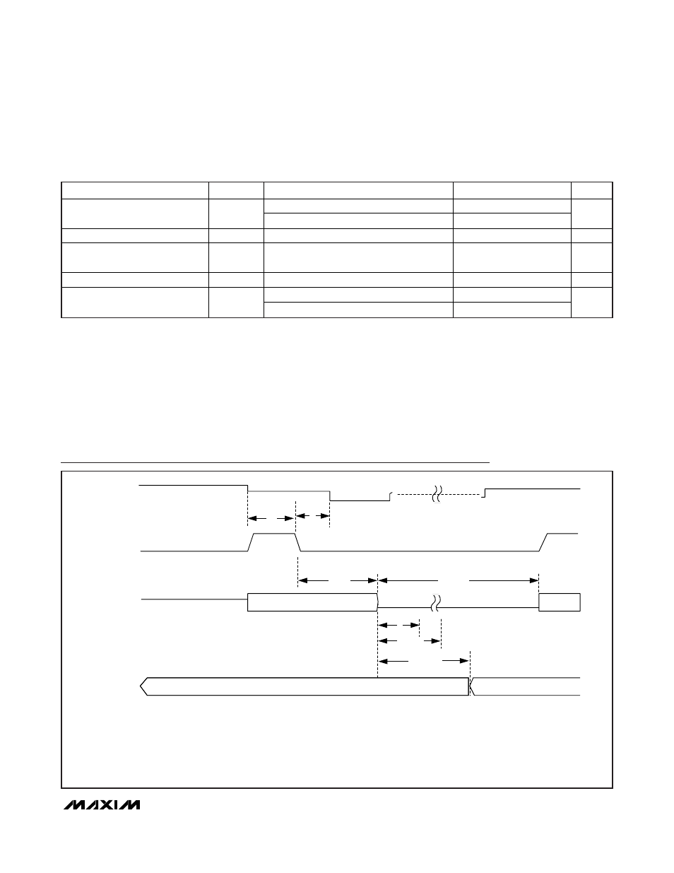
Timing Diagram
V
INP
- V
INN
V
OUTP
- V
OUTN
EXTERNAL
ADC DATA
t
ADC:ST
= EXTERNAL ADC SAMPLING TIME.
t
ADC:CT
= EXTERNAL ADC CONVERSION TIME.
DEN IS CONNECTED TO V
CC
FOR DIFFERENTIAL OUTPUT.
NOTE: THIS TIMING DIAGRAM IS APPLICABLE FOR SINGLE-ENDED AND DIFFERENTIAL OUTPUT CONFIGURATIONS.
SEN
t
S
t
DEL
t
OUT
t
ADC:ST
DATA VALID
t
ADC:CT
t
REC
t
HOLD
VOLTAGE INVALID