Ds1843 fast sample-and-hold circuit, Dc electrical characteristics – Rainbow Electronics DS1843 User Manual
Page 2
DS1843
Fast Sample-and-Hold Circuit
2
_______________________________________________________________________________________
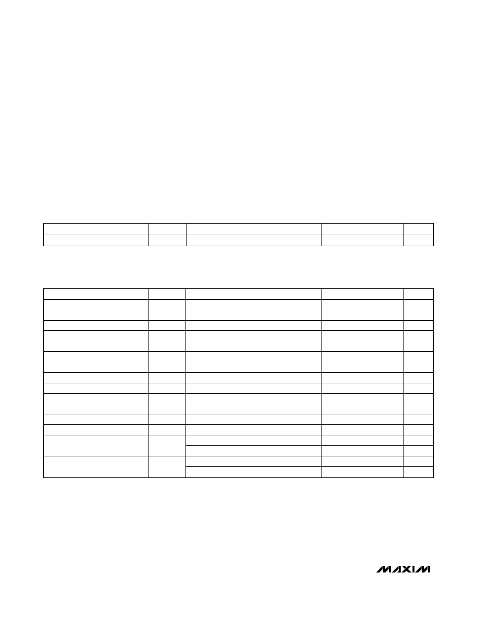
ABSOLUTE MAXIMUM RATINGS
RECOMMENDED OPERATING CONDITIONS
(T
A
= -40°C to +85°C, unless otherwise noted.)
Stresses beyond those listed under “Absolute Maximum Ratings” may cause permanent damage to the device. These are stress ratings only, and functional
operation of the device at these or any other conditions beyond those indicated in the operational sections of the specifications is not implied. Exposure to
absolute maximum rating conditions for extended periods may affect device reliability.
Voltage Range on V
CC
.............................................-0.5V to +6V
Voltage Range on V
OUTP
, V
OUTN
,
V
INP
, V
INN
, SEN, DEN ............................-0.5V to (V
CC
+ 0.5V)*
Operating Temperature Range ...........................-40°C to +85°C
Storage Temperature Range .............................-55°C to +125°C
Soldering Temperature ..............................................Refer to the
IPC/JEDEC J-STD-020 Specification.
PARAMETER
SYMBOL
CONDITIONS
MIN
TYP
MAX
UNITS
Supply Voltage
V
CC
(Note 1)
+2.97
+5.5
V
DC ELECTRICAL CHARACTERISTICS
(V
CC
= +2.97V to +5.5V, T
A
= -40°C to +85°C, unless otherwise noted.)
PARAMETER SYMBOL
CONDITIONS
MIN
TYP
MAX
UNITS
Supply Current
I
CC
(Note
1)
5.7 9 mA
Input Capacitance
C
IN
All pins (Note 2)
7
pF
Sample Capacitance
C
S
V
INN
and V
INP
(Note 2)
5
pF
Logic-Input Low
V
IL
SEN and DEN inputs
0.3 x
V
CC
V
Logic-Input High
V
IH
SEN and DEN inputs
0.7 x
V
CC
V
Input Leakage
I
IN
V
INN
or V
INP,
SEN = 0
1
μA
Input Voltage
V
IN
V
IN
= V
INP
- V
INN
0
1.0
V
Output Voltage
V
OUT
V
OUT
= V
OUTP
- V
OUTN
; 100k
load on
each output pin
0 1.0
V
Output Impedance
R
OUTMAX
(Note
2)
1
1.3
k
Output Capacitive Load
C
OUT
Capacitance for stable operation
50
pF
V
CC
= 2.9V, 1μs sample time, V
IN
= 6mV
3.6
6.1
mV
Total Input Referenced Voltage
Offset: Differential
V
OS-DIFF
Voltco (V
CC
= 2.9V to 5.5V)
1
mV/V
V
CC
= 2.9V, 1μs sample time, V
IN
= 6mV
3.4
8
mV
Total Input Referenced Voltage
Offset: Single-Ended
V
OS-SE
Voltco (V
CC
= 2.9V to 5.5V)
1
mV/V
*
Subject to not exceeding +6V.