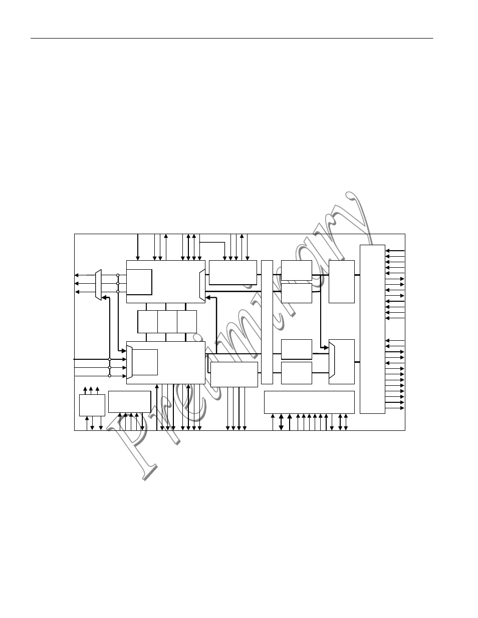
Description, Block diagram, Figure 1–1 block diagram – Rainbow Electronics DS3164 User Manual
Page 3: Applications, Access concentrators, Multi-service access platforms, Atm and frame relay equipment, Routers and switches, Sonet/sdh adm, Digital cross connect
Maxim/Dallas Semiconductor Confidential
Product Preview:
DS3161,2,3,4
Rev 1.6
3 of 12
022604
DESCRIPTION
The DS316x Multi-port PHYs map ATM cells and/or packets into as many as four DS3/E3 data streams.
Dedicated cell processor and packet processor blocks prepare outgoing cells or packets for transmission
and check incoming cells or packets upon arrival. Built-in DS3/E3 framers transmit and receive
cell/packet data in properly formatted M23 DS3, C-bit DS3, G.751 E3 or G.832 E3 data streams. PLCP
framers provide legacy ATM transmission-convergence support. With integrated hardware support for
both cells and packets, the DS316x PHYs enable high-density universal line cards for unchannelized
DS3/E3.
1 BLOCK
DIAGRAM
Figure 1–1 Block Diagram
T
LC
LK
n
TSOFn / TI
OH
Mn
T
D
A
T
n
T
D
E
N
n
/
T
G
C
LK
n
T
P
O
H
n
T
P
O
H
G
C
LK
n
T
P
O
H
SOFn
8KREF
I
T
O
H
n
T
O
H
G
C
L
K
n
TOH
S
OFn
TMEI
System
Interface
TSCLK
TADR[4:0]
TDATA[31:0]
TPRTY*
TEN*
TPXA
TDXA[4:1]
TSOX
TEOP
TSX
TMOD[1:0]
TERR
TSPA
Tx
FIFO
Tx
PLCP/DSS/FRAC
Formatter
Tx Cell
Processor
TPOSn / TNRZn
DS3 / E3
Transmit
Formatter
B3ZS/
HDB3
Encoder
TNEGn / TOHMn
Tx Packet
Processor
TCLKn
Fr
am
er
D
ia
gnosti
c
Loo
pback
System
In
ter
fac
e
Loo
pback
L
in
e
Fa
cility
L
o
op
ba
ck
Fr
am
er
Payl
oa
d
Loo
pback
Trail
Trace
Buffer
HDLC
FEAC
BERT
RSCLK
RADR[4:0]
RDATA[31:0]
RPRTY*
REN*
RPXA
RDXA[4:1]
RSOX
REOP
RSX
RVAL
RMOD[1:0]
RERR
Rx
FIFO
Rx Packet
Processor
DS3 / E3
Receive
Framer
B3ZS/
HDB3
Decoder
RPOSn / RNRZn
Rx
PLCP/DSS/FRAC
Framer
Rx Cell
Processor
RNEGn / RLCVn / ROHMn
RCLKn
Microprocessor
Interface
IEEE P1149.1
JTAG Test
Access Port
Clock
Rate
Adapter
n = port #
CLK
A
CLKB
REF
C
LK
R
D
A
T
n
R
D
EN
n / RG
C
LK
n
R
S
O
F
n
RL
CLKn
R
O
H
n
RE
CU
R
O
H
G
C
L
K
n
RO
HSOF
n
JT
D
O
JT
D
I
JT
C
LK
JT
RST
*
JT
M
S
R
P
O
H
n
R
P
O
H
G
C
LK
n
RPO
H
S
O
F
n
8KREFO
A
LE
C
S
*
R
D
*/
D
S
*
WR
*/
R
/W
*
M
O
T
R
S
T
*
INT
*
P
IO
A
n
PIOBn
D
[15
:0
]
A
[9:0
]
2 APPLICATIONS
• Access Concentrators
• Multi-Service Access Platforms
• ATM and Frame Relay Equipment
• Routers and Switches
• SONET/SDH ADM
• Digital Cross Connect
• PDH Multiplexer/Demultiplexer