At83c24 – Rainbow Electronics AT83C24NDS User Manual
Page 5
5
4234F–SCR–10/05
AT83C24
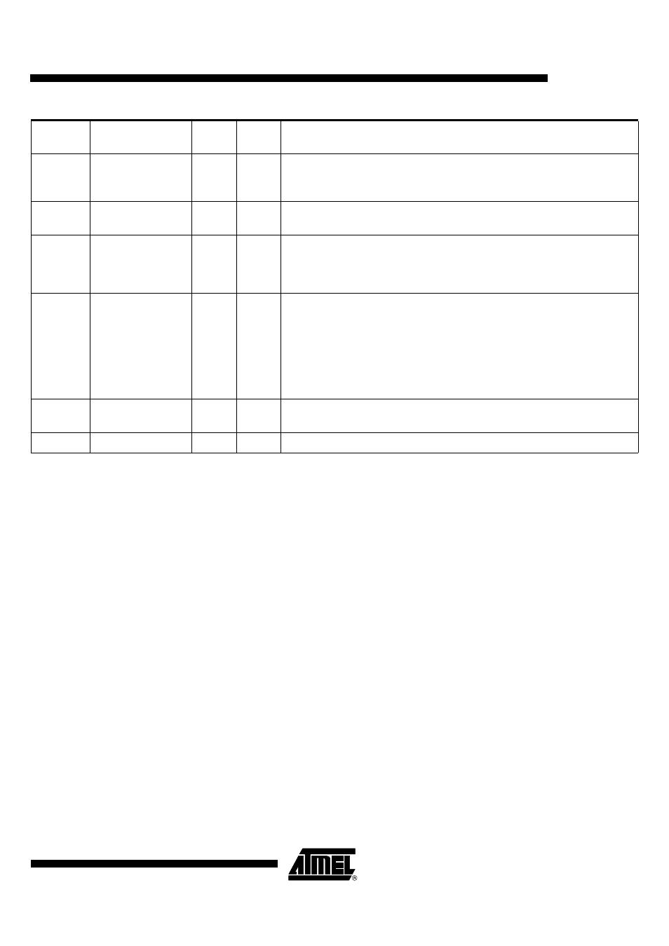
Note:
ESD Test conditions: 3 positive and 3 negative pulses on each pin versus GND. Pulses generated
according to Mil/STD 883 Class3. Recommended capacitors soldered on CVCC and VCC pins.
CVCC
8 kV+
PWR
Card Supply Voltage
CVCC is the programmable voltage output for the Card interface.
It must be connected to external decoupling capacitors (see page 34 and page 36).
CVCCin
8 kV+
PWR
Card Supply Voltage
This pin must be connected to CVCC.
DVCC
3 kV+
PWR
Digital Supply Voltage
Is internally generated and used to supply the digital core.
This pin has to be connected to an external capacitor of 100 nF and should not be
connected to other devices.
EVCC
3 kV+
PWR
Extra Supply Voltage (Microcontroller power supply)
EVCC is used to supply the internal level shifters of host interface pins.
EVCC voltage can be supplied from the external EVCC pin connected to the host power
supply.
If EVCC cannot be connected to the host power supply, it must be tied to an external
capacitor. EVCC voltage can be generated internally by an automatic follow up of the
logic high level on the I/O pin. In this configuration, connect a 100 nF + 100kOhms in
parallel between EVCC pin and VSS pin.
CVSS
8 kV+
GND
DC/DC Ground
CVSS is used to sink high shunt currents from the external coil.
VSS
GND
Ground
Table 1. Ports Description (Continued)
Pad Name
Pad Internal
Power Supply
ESD
Limits
Pad
Type
Description