At83c24 – Rainbow Electronics AT83C24NDS User Manual
Page 33
33
4234F–SCR–10/05
AT83C24
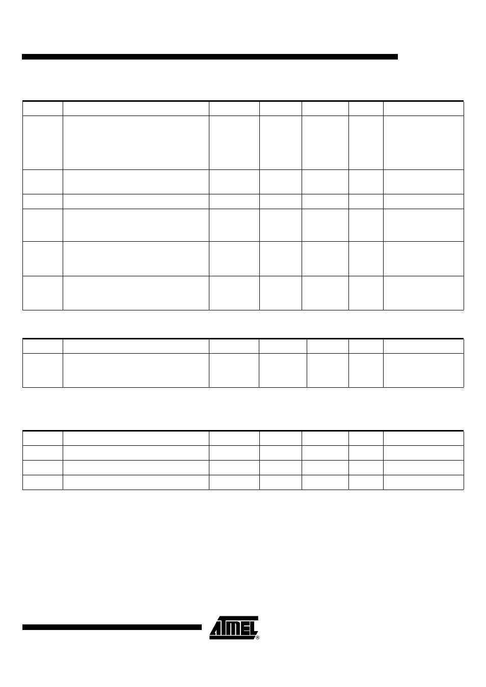
Table 25. Smart Card RST (CRST pin)
Symbol
Parameter
Min
Typ
Max
Unit
Test Conditions
V
OL
Output Low-voltage
0
0
0.12 x CVCC
0.4
0.2
V
I
OL
= -20 µA
CLASS
A&B&C
I
OL
= -200 µA
CLASS A
I
OL
= -200 µA
CLASS
B&C
V
OH
Output High Voltage
0.9*CVCC
CVCC
V
I
OH
= 200 µA
CLASS A&B&C
I
OS
Output High Current
-15
+15
mA
Short to GND or CVCC
t
R
t
F
Rise and Fall time
0.1
µs
C
L
= 30pF
measurement between
10% and 90% of CVCC
Low level voltage stability
(taking into account PCB design)
-0.25
0.50V
0.30V
0.30V
V
CLASS A
CLASS B
CLASS C
High level voltage stability
(taking into account PCB design)
4.2
2.35
CVCC-0.4
CVCC+0.25
V
CLASS A
CLASS B
CLASS C
Table 26. Card Presence
Symbol
Parameter
Min
Typ
Max
Unit
Test Conditions
R
CPRES
CPRES weak pull-up output current
300
330
360
κΩ
Short to VSS
PULLUP = 1:
Internal pull-up active
Table 27. TWI (SDA, SCL pins)
Symbol
Parameter
Min
Typ
Max
Unit
Test Conditions
t
SU;DAT
Data set-up time
20
10
ns
Not tested
t
HD;DAT
Data hold time
10
0
ns
Not tested
t
fDA
Fall time on SDA signal
50
ns
Not tested