At83c24 – Rainbow Electronics AT83C24NDS User Manual
Page 4
4
4234F–SCR–10/05
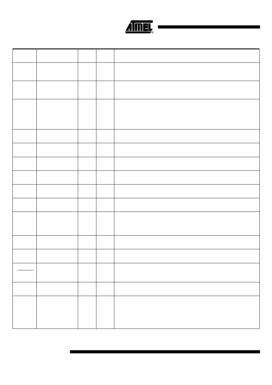
AT83C24
SDA
VCC
3 kV
I/O
open-
drain
Microcontroller Interface Function
TWI serial data
SCL
VCC
3 kV
I/O
open-
drain
Microcontroller Interface Function
TWI serial clock
I/O
EVCC
3 kV
I/O
Microcontroller Interface Function
Copy of CIO pin and high level reference for EVCC.
An external pull up to EVCC is needed on IO pin.
I/O is the reference level for EVCC if EVCC is connected to a capacitor.
This feature is unused if EVCC is connected to VCC.
C4
EVCC
3 kV
I/O
(pull-up)
Microcontroller Interface Function
Copy of Card CC4.
C8
EVCC
3 kV
I/O
(pull-up)
Microcontroller Interface Function
Copy of Card CC8.
CLK
EVCC
3 kV
I
Microcontroller Interface Function
Master Clock
CIO
CVCC
8 kV+
I/O
(pull-up)
Smart card interface function
Card I/O
CC4
CVCC
8 kV+
I/O
(pull-up)
Smart card interface function
Card C4
CC8
CVCC
8 kV+
I/O
(pull-up)
Smart card interface function
Card C8
CPRES
VCC
8 kV+
I
(pull-up)
Smart card interface function
Card presence
An internal Pull-up to VCC can be activated in the pad if necessary using PULLUP bit
(CONFIG1 register).
CCLK
CVCC
8 kV+
O
Smart card interface function
Card clock
CRST
CVCC
8 kV+
O
Smart card interface function
Card reset
CMDVCC
EVCC
3 kV+
I
(pull-up)
Microcontroller Interface Function:
Activation/Shutdown of the smart card Interface.
VCC
3 kV+
PWR
Supply Voltage
V
CC
is used to power the internal voltage regulators and I/O buffers.
LI
3 kV+
PWR
DC/DC Input
LI must be tied to VCC pin through an external coil (typically 4.7
μH) and provides the
current for the charge pump of the DC/DC converter.
It may be directly connected to VCC if the step-up converter is not used (see STEPREG
bit in CONFIG4 register and see minimum VCC values in Table 20 (class A) and
Table 21 (class B)).
Table 1. Ports Description (Continued)
Pad Name
Pad Internal
Power Supply
ESD
Limits
Pad
Type
Description