Pin description, Pinouts (top view), Signals – Rainbow Electronics AT83C24NDS User Manual
Page 3: At83c24
3
4234F–SCR–10/05
AT83C24
Pin Description
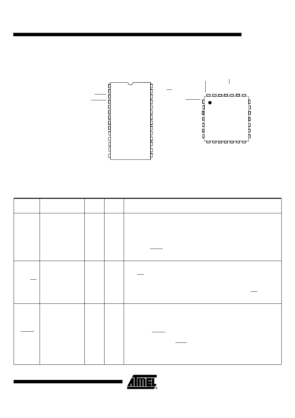
Pinouts (Top View)
28-pin SOIC Pinout
QFN28 pinout
Note:
1. NC = Not Connected
2. SOIC and QFN packages are available for
AT83C24 and for AT83C24NDS
Signals
A1
A2
A0
1
EVCC
CCLK
CRST
SCL
VCC
RESET
CVSS
CVCCin
I/O
CLK
2
3
4
5
6
7
8
9
10
28
27
26
25
24
23
22
21
20
19
LI
PRES/INT
DVCC
VSS
SDA
CPRES
12
18
17
11
C8
CIO
C4
16
15
CC8
CMDVCC
CC4
1
VSS
V
CC
CVSS
LI
2
3
4
5
6
7
8
9 10 11 12 13 14
16
15
17
18
19
20
21
22
23
24
25
26
27
28
TOP VIEW
QFN 28
CIO
CC
8
CVCCin
CRS
T
CP
RE
S
CC4
CC
L
K
CMDVCC
RES
E
T
DV
C
C
C8
CL
K
PRES/INT
C4
/CK
/CK
/RST
A0
/RST
/3V
/3V
CVCC
CVCC
SDA
SCL
A1
A2
I/
O
EVCC
13
14
NC
NC
NC
NC
Table 1. Ports Description
Pad Name
Pad Internal
Power Supply
ESD
Limits
Pad
Type
Description
A2/CK-
A1/RST-
A0/3V
EVCC
3 kV
I
Microcontroller Interface Function:
TWI bus slave address selection input.
A2/CK and A1/RST pins are respectively connected to CCLK and CRST signals in
“transparent mode” (see page 17 ).
A0/3V is used for hardware activation to select CVCC voltage (3V or 5V).
The slave address of the device is based on the value present on A2, A1, A0 on the
rising edge of RESET pin (see Table 2). In fact, the address is taken internally at the 11th
CLK rising edge.
PRES/INT
EVCC
3 kV
O
open-
drain
Microcontroller Interface Function:
Depending on IT_SEL value (see CONFIG4 register),
PRES/INT outputs card presence status or interruptions (page 9)
An internal Pull-up (typ 330k
Ω,see Table 18)to EVCC can be activated in the pad if
necessary using INT_PULLUP bit (CONFIG4 register).
Remark: during power up and before registers configuration, the PRES/INT signal must
be ignored.
RESET
VCC
3 kV
I/O
open-
drain
Microcontroller Interface Function:
•
Power-on reset
•
A low level on this pin keeps the AT83C24 under reset even if applied on power-on.
It also resets the AT83C24 if applied when the AT83C24 is running (see Power
monitoring §).
•
Asserting RESET when the chip is in Shut-down mode returns the chip to normal
operation.
•
AT83C24 is driving the Reset pin Low on power-on-reset or if power fail on V
CC
or
DVCC (see POWERMON bit in CONFIG4 register), this can be used to reset or
interrupt other devices. After reset, AT83C24 needs to be reconfigured before
starting a new card session.