Electrical characteristics, Absolute maximum ratings, Dc parameters for standard voltage – Rainbow Electronics T89C5115 User Manual
Page 92
92
T89C5115
4128A–8051–04/02
Electrical Characteristics
Absolute Maximum Ratings
DC Parameters for Standard Voltage
T
A
= -40
°
C to +85
°
C; V
SS
= 0V; V
CC
= 5V
±
10%; F = 0 to 40 MHz
Notes:
1. Operating I
CC
is measured with all output pins disconnected; XTAL1 driven with T
CLCH
, T
CHCL
= 5 ns (see Figure 44.), V
IL
=
V
SS
+ 0.5V, V
IH
= V
CC
- 0.5V; XTAL2 N.C.; RST = V
CC
. I
CC
would be slightly higher if a crystal oscillator used (see Figure 41.).
2. Idle I
CC
is measured with all output pins disconnected; XTAL1 driven with T
CLCH
, T
CHCL
= 5 ns, V
IL
= V
SS
+ 0.5V, V
IH
= V
CC
-
0.5V; XTAL2 N.C; Port 0 = V
CC
; RST = V
SS
(see Figure 42.).
3. Power-down I
CC
is measured with all output pins disconnected; XTAL2 NC.; RST = V
SS
(see Figure 43.). In addition, the
WDT must be inactive and the POF flag must be set.
4. Typicals are based on a limited number of samples and are not guaranteed. The values listed are at room temperature.
Ambiant Temperature Under Bias:
I = industrial ....................................................... -40
°
C to 85
°
C
Storage Temperature ................................... -65
°
C to + 150
°
C
Voltage on V
CC
from V
SS
......................................-0.5V to + 6V
Voltage on Any Pin from V
SS
....................-0.5V to V
CC
+ 0.2 V
Power Dissipation ............................................................. 1 W
Note:
Stresses at or above those listed under “Absolute
Maximum Ratings” may cause permanent damage to
the device. This is a stress rating only and functional
operation of the device at these or any other condi-
tions above those indicated in the operational
sections of this specification is not implied. Exposure
to absolute maximum rating conditions may affect
device reliability.
The power dissipation is based on the maximum
allowable die temperature and the thermal resistance
of the package.
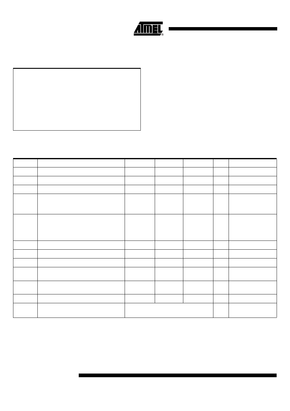
Table 68. DC Parameters in Standard Voltage
Symbol
Parameter
Min
Typ
(5)
Max
Unit
Test Conditions
V
IL
Input Low Voltage
-0.5
0.2 Vcc - 0.1
V
V
IH
Input High Voltage except XTAL1, RST
0.2 V
CC
+ 0.9
V
CC
+ 0.5
V
V
IH1
Input High Voltage, XTAL1, RST
0.7 V
CC
V
CC
+ 0.5
V
V
OL
Output Low Voltage, ports 1, 2, 3 and 4
(6)
0.3
0.45
1.0
V
V
V
I
OL
= 100
µ
A
I
OL
= 1.6 mA
I
OL
= 3.5 mA
V
OH
Output High Voltage, ports 1, 2, 3, 4
V
CC
- 0.3
V
CC
- 0.7
V
CC
- 1.5
V
V
V
I
OH
= -10
µ
A
I
OH
= -30
µ
A
I
OH
= -60
µ
A
V
CC
= 5V
±
10%
R
RST
RST Pulldown Resistor
50
90
200
k
Ω
I
IL
Logical 0 Input Current ports 1, 2, 3 and 4
-50
µ
A
Vin = 0.45V
I
LI
Input Leakage Current
±
10
µ
A
0.45V < Vin < V
CC
I
TL
Logical 1 to 0 Transition Current, ports 1, 2, 3
and 4
-650
µ
A
Vin = 2.0V
C
IO
Capacitance of I/O Buffer
10
pF
Fc = 1 MHz
T
A
= 25
°
C
I
PD
Power-down Current
160
350
µ
A
4.5V < V
CC
< 5.5V
(3)
I
CC
Power Supply Current
I
CCOP
= 0.7 Freq (MHz) + 3 mA
I
CCIDLE
= 0.6 Freq (MHz) + 2 mA
Vcc = SS
(1) (2)