Overview of fm0 operations – Rainbow Electronics T89C5115 User Manual
Page 31
31
T89C5115
4128A–8051–04/02
Overview of FM0
Operations
The CPU interfaces to the Flash memory through the FCON register and AUXR1
register.
These registers are used to:
•
Map the memory spaces in the adressable space
•
Launch the programming of the memory spaces
•
Get the status of the flash memory (busy/not busy)
Mapping of the Memory Space
By default, the user space is accessed by MOVC instruction for read only. The column
latches space is made accessible by setting the FPS bit in FCON register. Writing is
possible from 0000h to 3FFFh, address bits 6 to 0 are used to select an address within a
page while bits 14 to 7 are used to select the programming address of the page.
Setting FPS bit takes precedence on the EEE bit in EECON register.
The other memory spaces (user, extra row, hardware security) are made accessible in
the code segment by programming bits FMOD0 and FMOD1 in FCON register in accor-
dance with Table 20. A MOVC instruction is then used for reading these spaces.
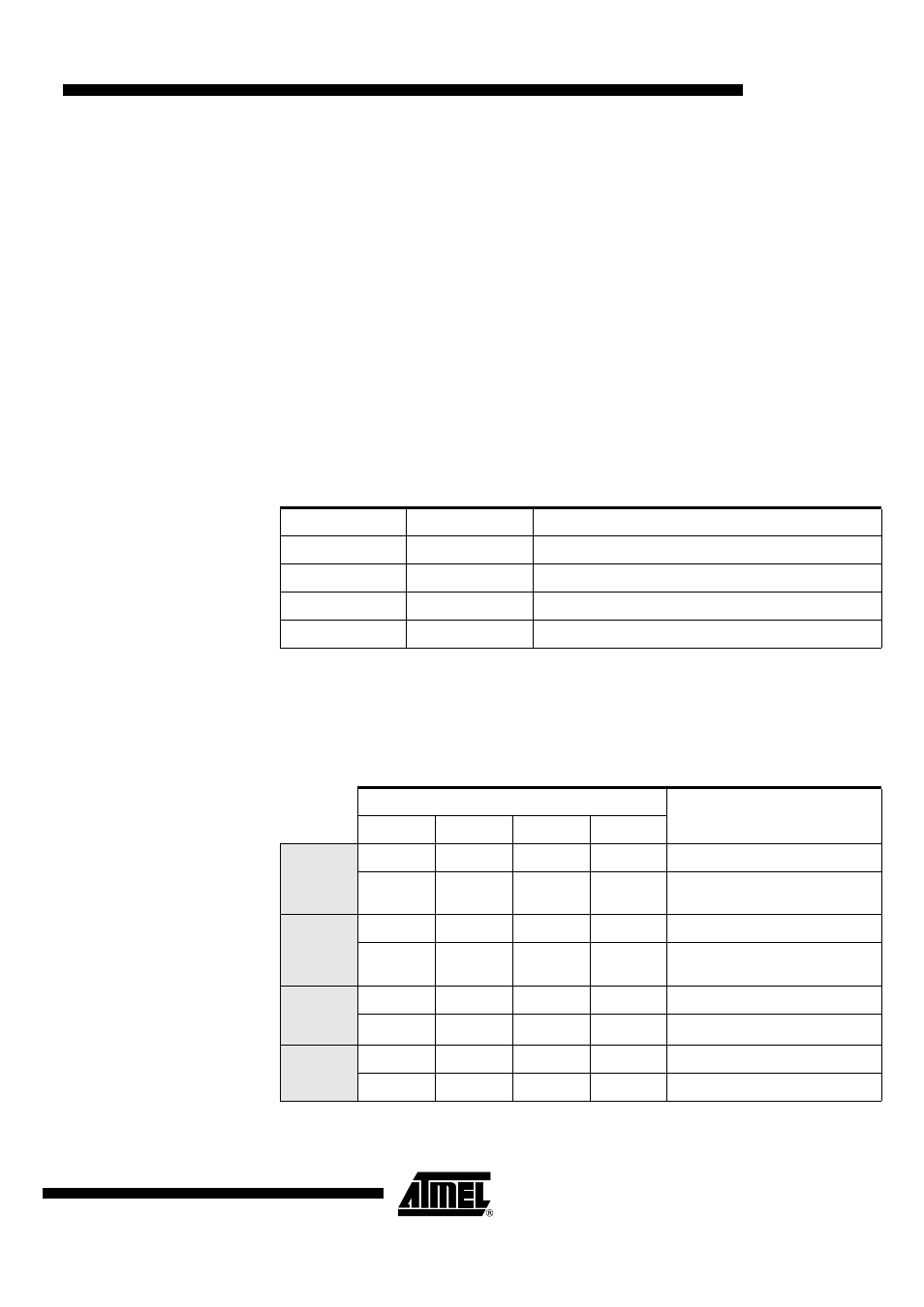
Table 20. FM0 Blocks Select Bits
Launching Programming
FPL3:0 bits in FCON register are used to secure the launch of programming. A specific
sequence must be written in these bits to unlock the write protection and to launch the
programming. This sequence is 5xh followed by Axh. Table 21 summarizes the memory
spaces to program according to FMOD1:0 bits.
Table 21. Programming Spaces
Note:
The sequence 5xh and Axh must be executing without instructions between them other-
wise the programming is aborted.
FMOD1
FMOD0
FM0 Adressable space
0
0
User (0000h-3FFFh)
0
1
Extra Row(FF80h-FFFFh)
1
0
Hardware Security Byte (0000h)
1
1
reserved
Write to FCON
Operation
FPL3:0
FPS
FMOD1
FMOD0
User
5
X
0
0
No action
A
X
0
0
Write the column latches in user
space
Extra Row
5
X
0
1
No action
A
X
0
1
Write the column latches in extra row
space
Hardware
Security
Byte
5
X
1
0
No action
A
X
1
0
Write the fuse bits space
Reserved
5
X
1
1
No action
A
X
1
1
No action