Adc converter operation – Rainbow Electronics T89C5115 User Manual
Page 79
79
T89C5115
4128A–8051–04/02
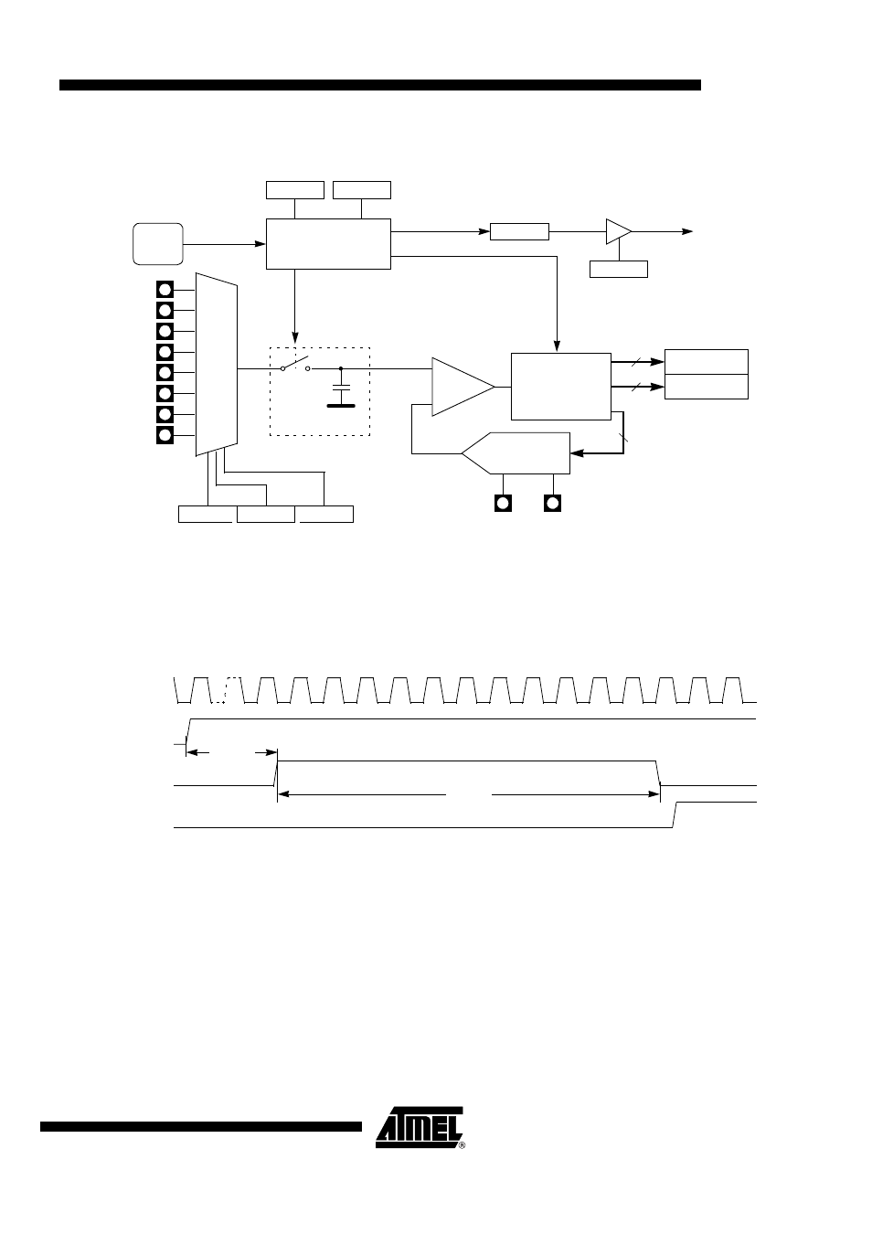
Figure 36. ADC Description
Figure 37 shows the timing diagram of a complete conversion. For simplicity, the figure
depicts the waveforms in idealized form and do not provide precise timing information.
For ADC characteristics and timing parameters refer to the Section “AC Characteristics”
of the T89C5115 datasheet.
Figure 37. Timing Diagram
Note:
Tsetup min = 4 us
Tconv=11 clock ADC = 1sample and hold + 10 bit conversion
The user must ensure that 4 us minimum time between setting ADEN and the start of the first conversion.
ADC Converter
Operation
A start of single A/D conversion is triggered by setting bit ADSST (ADCON.3).
After completion of the A/D conversion, the ADSST bit is cleared by hardware.
The end-of-conversion flag ADEOC (ADCON.4) is set when the value of conversion is
available in ADDH and ADDL, it must be cleared by software. If the bit EADC (IEN1.1) is
set, an interrupt occur when flag ADEOC is set (see Figure 39). Clear this flag for re-
arming the interrupt.
The bits SCH0 to SCH2 in ADCON register are used for the analog input channel
selection.
AN0/P1.0
AN1/P1.1
AN2/P1.2
AN3/P1.3
AN4/P1.4
AN5/P1.5
AN6/P1.6
AN7/P1.7
000
001
010
011
100
101
110
111
SCH2
ADCON.2
SCH0
ADCON.0
SCH1
ADCON.1
ADC
CLOCK
ADEN
ADCON.5
ADSST
ADCON.3
ADEOC
ADCON.4
ADC
Interrupt
Request
EADC
IEN1.1
CONTROL
AVSS
Sample and Hold
ADDH
VAREF
R/2R DAC
VAGND
8
10
+
-
ADDL
2
SAR
ADCIN
ADEN
ADSST
ADEOC
T
SETUP
T
CONV
CLK