Program/code memory, Flash memory architecture – Rainbow Electronics T89C5115 User Manual
Page 29

29
T89C5115
4128A–8051–04/02
Program/Code
Memory
The T89C5115 implement 16-KB of on-chip program/code memory.
The Flash memory increases EPROM and ROM functionality by in-circuit electrical era-
sure and programming. Thanks to the internal charge pump, the high voltage needed for
programming or erasing Flash cells is generated on-chip using the standard VDD volt-
age. Thus, the Flash Memory can be programmed using only one voltage and allows In-
System Programming commonly known as ISP. Hardware programming mode is also
available using specific programming tool.
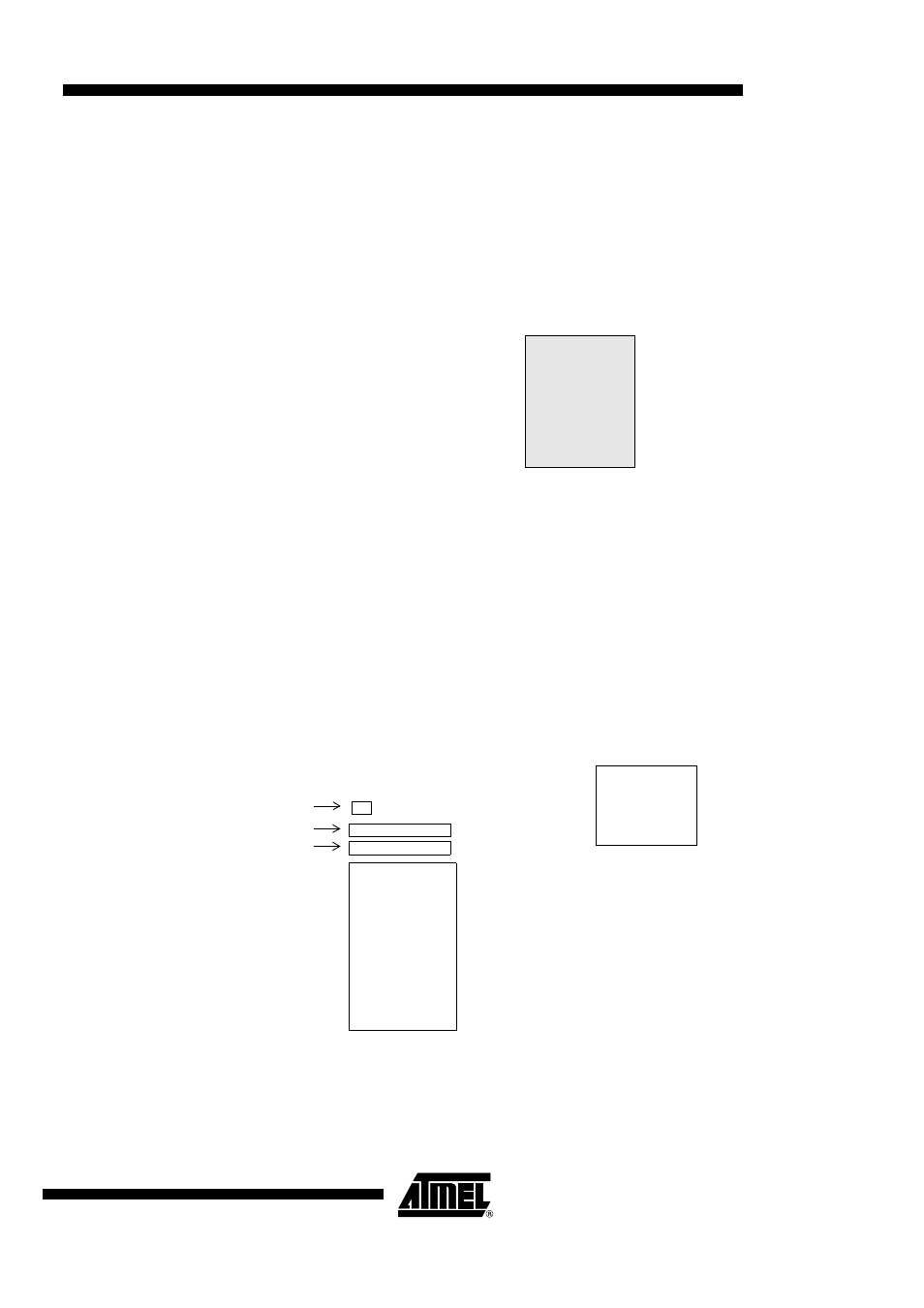
Figure 10. Program/Code Memory Organization
Flash Memory
Architecture
T89C5115 features two on-chip flash memories:
•
Flash memory FM0:
containing 16-KB of program memory (user space) organized into pages 128 bytes
•
Flash memory FM1:
2K Bytes for boot loader and Application Programming Interfaces (API).
The FM0 can be program by both parallel programming and Serial In-System Program-
ming (ISP) whereas FM1 supports only parallel programming by programmers. The ISP
mode is detailed in the "In-System Programming" section.
All Read/Write access operations on Flash Memory by user application are managed by
a set of API described in the "In-System Programming" section.
Figure 11. Flash Memory Architecture
0000h
16-KB
3FFFh
internal
Flash
3FFFh
16-KB
Flash memory
FM0
0000h
Hardware Security (1 byte)
Column Latches (128 bytes)
user space
Extra Row (128 bytes)
2K Bytes
Flash memory
FM1
boot space
FFFFh
F800h
FM1 mapped between FFFFh and
F800h when bit ENBOOT is set in
AUXR1 register
