Table, Table 39), Table 39 – Rainbow Electronics T89C5115 User Manual
Page 60

60
T89C5115
4128A–8051–04/02
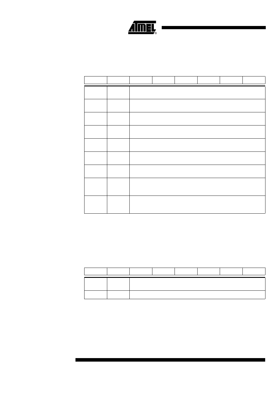
Table 38. T2MOD Register
T2MOD (S:C9h)
Timer 2 Mode Control Register
Reset Value = XXXX XX00b
Not bit addressable
Table 39. TH2 Register
TH2 (S:CDh)
Timer 2 High Byte Register
Reset Value = 0000 0000b
Not bit addressable
7
6
5
4
3
2
1
0
-
-
-
-
-
-
T2OE
DCEN
Bit
Number
Bit
Mnemonic
Description
7
-
Reserved
The value read from this bit is indeterminate. Do not set this bit.
6
-
Reserved
The value read from this bit is indeterminate. Do not set this bit.
5
-
Reserved
The value read from this bit is indeterminate. Do not set this bit.
4
-
Reserved
The value read from this bit is indeterminate. Do not set this bit.
3
-
Reserved
The value read from this bit is indeterminate. Do not set this bit.
2
-
Reserved
The value read from this bit is indeterminate. Do not set this bit.
1
T2OE
Timer 2 Output Enable bit
Clear to program P1.0/T2 as clock input or I/O port.
Set to program P1.0/T2 as clock output.
0
DCEN
Down Counter Enable bit
Clear to disable Timer 2 as up/down counter.
Set to enable Timer 2 as up/down counter.
7
6
5
4
3
2
1
0
-
-
-
-
-
-
-
-
Bit
Number
Bit
Mnemonic
Description
7-0
High Byte of Timer 2.
