Pin description, Typical operating characteristics (continued) – Rainbow Electronics MAX9995 User Manual
Page 8
MAX9995
Dual, SiGe, High-Linearity, 1700MHz to 2200MHz
Downconversion Mixer with LO Buffer/Switch
8
_______________________________________________________________________________________
PIN
NAME
FUNCTION
1
RFMAIN
Main Channel RF Input. Internally matched to 50
Ω. Requires an input DC-blocking capacitor.
2
TAPMAIN
Main Channel Balun Center Tap. Connect a 0.033µF capacitor from this pin to the board ground.
3, 5, 7, 12, 20, 22,
24, 25, 26, 34
GND
Ground
4, 6, 10, 16, 21, 30,
36
V
CC
Power Supply. Connect bypass capacitors as close to the pin as possible (see the Typical
Application Circuit).
8
TAPDIV
Diversity Channel Balun Center Tap. Connect a 0.033µF capacitor from this pin to the ground.
9
RFDIV
Diversity Channel RF Input. Internally matched to 50
Ω. Requires an input DC-blocking capacitor.
11
IFD_SET
IF Diversity Amplifier Bias Control. Connect a 1.2k
Ω resistor from this pin to ground to set the
bias current for the diversity IF amplifier.
13, 14
IFD+, IFD-
Diversity Mixer Differential IF Output. Connect pullup inductors from each of these pins to V
CC
(see the Typical Application Circuit).
15
IND_EXTD
Connect a 10nH inductor from this pin to ground to increase the RF-IF and LO-IF isolation.
17
LO_ADJ_D
LO Diversity Amplifier Bias Control. Connect a 392
Ω resistor from this pin to ground to set the
bias current for the diversity LO amplifier.
18, 28
N.C.
No Connection. Not internally connected.
19
LO1
Local Oscillator 1 Input. This input is internally matched to 50
Ω. Requires an input DC-blocking
capacitor.
23
LOSEL
Local Oscillator Select. Set this pin to high to select LO1. Set to low to select LO2.
Pin Description
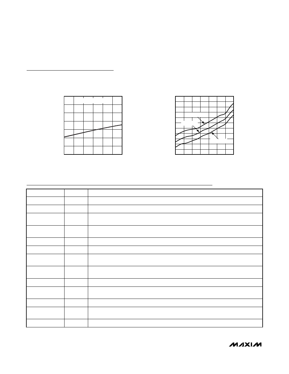
LO RETURN LOSS vs. LO FREQUENCY
(LO INPUT UN SELECTED)
MAX9995 toc37
FREQUENCY (MHz)
RETURN LOSS (dB)
1900
1800
1700
1600
1500
30
25
20
15
10
5
0
35
1400
2000
P
LO
= -3dBm TO +3dBm
310
330
325
320
315
340
335
360
355
350
345
365
-20
-5
10
25
40
55
70
85
SUPPLY CURRENT vs. TEMPERATURE (T
C
)
MAX9995 toc38
TEMPERATURE (°C)
SUPPLY CURRENT (mA)
V
CC
= 5.25V
V
CC
= 4.75V
V
CC
= 5.0V
Typical Operating Characteristics (continued)
(Typical Application Circuit, V
CC
= 5.0V, P
RF
= -5dBm, P
LO
= 0dBm, LO is low-side injected for a 200MHz IF, T
C
= +25°C.)