Electrical characteristics (continued) – Rainbow Electronics MAX17480 User Manual
Page 9

MAX17480
AMD 2-/3-Output Mobile Serial
VID Controller
_______________________________________________________________________________________
9
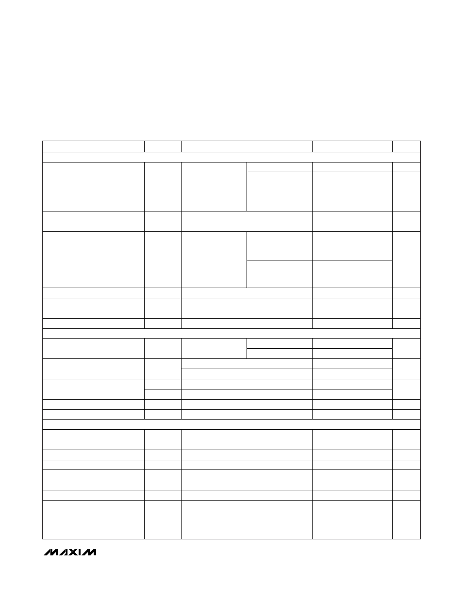
ELECTRICAL CHARACTERISTICS (continued)
(Circuit of Figure 2, V
IN
= 12V, V
CC
= V
DD
= V
IN3
= SHDN = PGD_IN = 5V, V
DDIO
= 1.8V, OPTION = GNDS_ = AGND = PGND,
FBDC_ = FBAC_ = OUT3 = CSP_ = CSN_ = 1.2V, all DAC codes set to the 1.2V code, T
A
= -40°C to +105°C, unless otherwise
noted. Typical values are at T
A
= +25
°C.) (Note 5)
PARAMETER
SYMBOL
CONDITIONS
MIN
TYP
MAX
UNITS
FAULT DETECTION
PWM mode
250
350
mV
Output Overvoltage Trip
Threshold
(SMPS1 and SMPS2 Only)
V
OVP_
Measured at
FBDC_, rising edge
Skip mode and
output have not
reached the
regulation voltage
1.80 1.90 V
Output Undervoltage Protection
Trip Threshold
V
UVP
Measured at FBDC_ or OUT3 with respect
to unloaded output voltage
-450 -350 mV
Lower threshold,
falling edge
(undervoltage)
-350 -250
PWRGD Threshold
Measured at FBDC_
or OUT3 with respect
to unloaded output
voltage, 15mV
hysteresis (typ)
Upper threshold,
rising edge
(overvoltage)
+150 +250
mV
PWRGD, Output Low Voltage
I
SINK
= 4mA
0.4
V
VRHOT Trip Threshold
Measured at THRM, with respect to V
CC,
falling edge, 115mV hysteresis (typ)
29.5 30.5 %
VRHOT, Output Low Voltage
I
SINK
= 4mA
0.4
V
GATE DRIVERS
High state (pullup)
2.5
DH_ Gate-Driver On-Resistance
R
ON(DH
_
)
BST_ - LX_ forced to
5V (Note 4)
Low state (pulldown)
2.5
DL_, high state
2.0
DL_ Gate-Driver On-Resistance
R
ON(DL
_
)
DL_, low state
0.6
t
DH
_
DL
DH_ low to DL_ high
9
35
Dead Time
t
DL
_
DH
DL_ low to DH_ high
9
35
ns
Internal BST1, BST2 Switch R
ON
BST1, BST2 to V
DD
, I
BST1
= I
BST2
= 10mA
20
Internal BST3 Switch R
ON
BST3 to V
DD
, I
BST3
= 10mA
20
2-WIRE I
2
C BUS LOGIC INTERFACE
SVI Logic-Input Threshold
SVC, SVD, rising edge, hysteresis = 0.14 x
V
DDIO
(V)
0.3 x
V
DDIO
0.7 x
V
DDIO
V
SVC Clock Frequency
f
SVC
3.4
MHz
START Condition Hold Time
t
SU;STA
160
ns
Repeated START Condition
Setup Time
t
SU;STA
160
ns
STOP Condition Setup Time
t
SU;STO
160
ns
Data Hold
t
HD;DAT
A master device must internally provide a
hold time of at least 300ns for the SVD signal
(referred to the V
IHMIN
of SVC signal) to bridge
the undefined region of SVC’s falling edge
70
ns
