Rainbow Electronics MAX17480 User Manual
Page 33

MAX17480
AMD 2-/3-Output Mobile Serial
VID Controller
______________________________________________________________________________________
33
Combined-Mode Current Balance
When the core SMPSs are configured in combined
mode (GNDS1 or GNDS2 pulled to V
DDIO
), the
MAX17480 current-mode architecture automatically
forces the individual phases to remain current bal-
anced. SMPS1 is the main voltage-control loop, and
SMPS2 maintains the current balance between the
phases. This control scheme regulates the peak induc-
tor current of each phase, forcing them to remain prop-
erly balanced. Therefore, the average inductor current
variation depends mainly on the variation in the current-
sense element and inductance value.
Peak Current Limit
The MAX17480 current-limit circuit employs a fast peak
inductor current-sensing algorithm. Once the current-
sense signal of the SMPS exceeds the peak current-limit
threshold, the PWM controller terminates the on-time.
See the
Core Peak Inductor Current Limit (ILIM12)
sec-
tion in the
Core SMPS Design Procedure
section.
Power-Up Sequence (POR, UVLO, PGD_IN)
Power-on reset (POR) occurs when V
CC
rises above
approximately 3V, resetting the fault latch and preparing
the controller for operation. The V
CC
undervoltage-lockout
(UVLO) circuitry inhibits switching until V
CC
rises above
4.25V (typ). The controller powers up the reference once
the system enables the controller V
CC
above 4.25V and
SHDN is driven high. With the reference in regulation, the
controller ramps the SMPS and NB voltages to the boot
voltage set by the SVC and SVD inputs:
The soft-start circuitry does not use a variable current
limit, so full output current is available immediately.
PWRGD becomes high impedance approximately 20µs
after the SMPS outputs reach regulation. The boot VID
is stored the first time PWRGD goes high. The
MAX17480 is in pulse-skipping mode during soft-start.
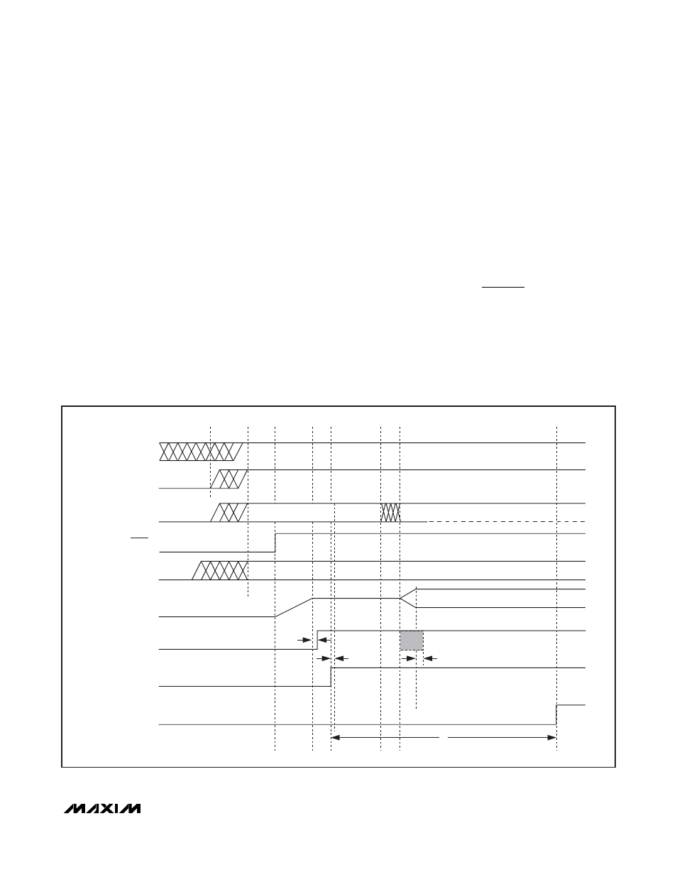
Figure 8 shows the MAX17480 startup sequence.
t
V
mV s
START
BOOT
=
(
)
1
/µ
20
µ
s
10
µ
s
20
µ
s
7
1
2
3
4
5
6
8
DC_IN
V
DDIO
SVC/SVD
GNDS1 OR GNDS2
(VDD_PLANE_STRAP)
SMPS V
OUT
PWRGD
PGD_IN
RESET_L
SHDN
BUS IDLE
2-BIT BOOT VID
SERIAL MODE
BLANK
HIGH-Z
Figure 8. Startup Sequence
