Page head, Page head clock and synchronization in system 6000, Causes of jitter – TC Electronic Broadcast 6000 User Manual
Page 57: How to detect jitter in the system
57
paGe Head
in dept
H
57
paGe Head
ClOCK and synCHrOnIzaTIOn In sysTem 6000
the clock from the incoming digital signal in order to be
synchronized to the transmitting device. In conventional
circuit designs the extracted clock is typically used directly
for the converters. This means that the jitter on the digital
interface is fed nearly unaltered to the converters and
therefore manifests as sampling jitter.
Causes of Jitter
There are several ways that jitter find it’s way into a digital
studio setup.
Noise induced on cables
A digital receiver typically detects a rising or a falling edge
on a digital signal at approx. halfway level. Due to finite
rise/fall times on the signal, noise then can disturb the
detection so the receiver detects the edges imprecisely.
Therefore, both noise and other interference imposed
on the signal line and the slope of the signal edge has
influence on the precision of the receiver. Some digital
formats are unbalanced (coaxial-S/PDIF) and others are
balanced (AES/EBU). The balanced signals are more
immune to induced noise due to the noise being treated
as a common mode signal, which is suppressed to some
extend in the receiving device.
Data jitter (or program jitter)
Data jitter is caused by high frequency loss in cables and
the nature of some digital formats (e.g. AES/EBU and S/
PDIF). Because the electrical data patterns are irregular
and changes all the time, a specific edge in the signal can
arrive at different times depending on the data pattern prior
to the edge. If there weren’t any high frequency loss in the
cable this wouldn’t be the case.
By using cables with incorrect impedance there will be a
non-ideal transmission line that potentially contributes to
the sloped edges and high frequency loss, and therefore
indirectly generates jitter. In this respect, unbalanced
formats (like S/PDIF) is often superior to its balanced
counterparts.
Optical formats
Some digital formats are optical (Toslink-S/PDIF and
ADAT) and they have a reputation of being bad formats
jitter wise. One of the reasons for this is that the most
common circuits used for converting between electrical and
optical signal are better at making a rising than a falling
edge. This causes asymmetries in the transferred digital
signal, which also contribute to data jitter.
Internal design
Every oscillator or PLL (phase locked loop) will be
uncertain about the time to some extent. (A PLL is typically
used to multiply frequencies or to filter a clock signal in
order to reduce jitter - jitter rejection).
This kind of basic incertainty is called intrinsic jitter and for
cheap designs it can be quite severe (there are examples
of up to 300ns peak where the limit for the AES format is 4
ns peak @ 48 kHz Fs, BW: 700 to 100 kHz [3]).
Devices that feature jitter rejection will typically be well
designed regarding intrinsic jitter as well.
Jitter accumulation
Jitter accumulation can happen in a chain of devices due
to intrinsic jitter PLUS jitter gain (see The clock design
on System 6000) in devices PLUS cable introduced jitter.
Every device and cable will add a bit of jitter and in the
end the jitter amount can get disturbing. There are ways to
overcome this potential problem (see Synchronization).
How to detect jitter in the system
How to detect sampling jitter
The higher rise/fall time of the program signal the more
sensitive it is to sample clock jitter and therefore one of
the best ways to analyze a converter performance jitter
wise is to apply a full-scale high frequency sine to the
converter. The sample clock jitter will then be modulated
onto the audio signal and it is now possible to measure
the jitter frequency spectrum by performing an FFT on the
converted audio signal.
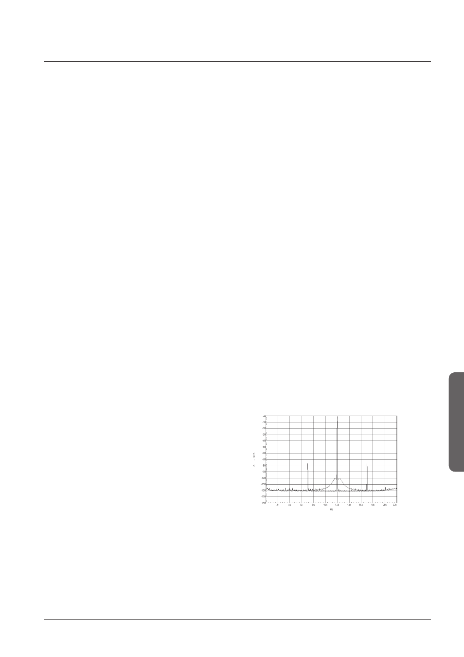
In Figure 1 the DAC has been converting a 12 kHz sine.
The two curves illustrate the difference with and without 5
kHz 3.5ns RMS jitter being applied on the digital interface.
In this example the device has no rejection of the jitter
appearing on the digital interface so it is nearly directly
transferred to the converter where it is modulated into the
audio signal. A conventional design like this is discussed in
more details later.
The two jitter spikes are at the frequencies 12 kHz +/- 5kHz
and the level approx. -80 dB corresponds to the 5kHz
3.5ns RMS jitter being applied. Sampling jitter (for jitter
frequencies below Fs/2) will appear symmetrically around
the sine being converted. Jitter frequencies above Fs/2 will
be modulated into the audio signal in a more complex way.
Another thing to notice on Figure 1 is that on the curve with
5kHz jitter there is also a tendency of some low frequency
< 2 kHz (note 12 kHz +/- 2 kHz) noise jitter. This might be
due to noise in the circuit generating the 5 kHz jitter.
Figure 1 FFT on a DAC. Measurement made on Audio
Precision System 2 Cascade using a 2k point FFT with 256
times average, and equiripple window. Two curves: Upper
with a 12kHz spike and two 12kHz +/- 5kHz spikes. Lower
only with a 12kHz spike.