Ml310 pm2 user i/o – Xilinx ML310 User Manual
Page 68
68
ML310 User Guide
1-800-255-7778
UG068 (v1.01) August 25, 2004
Chapter 2: ML310 Embedded Development Platform
R
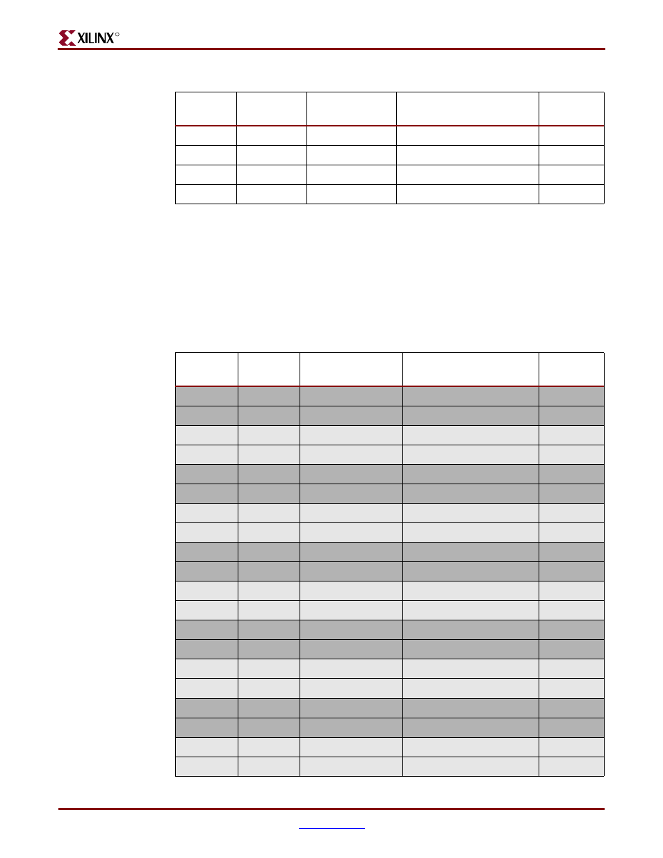
ML310 PM2 User I/O
The PM2 connector makes most of the LVDS pairs available to the user, along with single-
ended signals.
shows the pinout for the PM2 connector on the ML310.
F17
AK11
RXNPAD18
RXNPAD18_AK11
F18
AK12
RXPPAD18
RXPPAD18_AK12
F19
AK24
RXNPAD21
RXNPAD21_AK24
F20
AK25
RXPPAD21
RXPPAD21_AK25
Notes:
1. LVDS pairs are shown shaded; all other signals are single-ended.
2. LVDS pairs can also be used as single-ended I/O at 2.5V
3. NC indicates a “no connect” signal.
Table 2-31:
PM1 Pinout (Continued)
PM1 Pin
FPGA Pin
Pin Description
ML310 Schematic Net
FPGA Bank
V
CCO
Table 2-32:
PM2 Pinout
PM2 Pin
FPGA Pin
Pin Description
ML310 Schematic Net
FPGA Bank
V
CCO
A1
T5
IO_L89N_3
PM_IO_69
2.5V
A2
T6
IO_L89P_3
PM_IO_68
2.5V
A3
T3
IO_L88N_3
PM_IO_67
2.5V
A4
T4
IO_L88P_3
PM_IO_66
2.5V
A5
V3
IO_L58N_3
PM_IO_55
2.5V
A6
V4
IO_L58P_3
PM_IO_54
2.5V
A7
U7
IO_L56N_3
PM_IO_51
2.5V
A8
U8
IO_L56P_3
PM_IO_50
2.5V
A9
V7
IO_L53N_3
PM_IO_45
2.5V
A10
V8
IO_L53P_3
PM_IO_44
2.5V
A11
AC15
IO_L67P_4
PM_IO_72
2.5V
A12
AB15
IO_L67N_4
PM_IO_73
2.5V
A13
AA4
IO_L48P_3
PM_IO_34
2.5V
A14
AA3
IO_L48N_3
PM_IO_35
2.5V
A15
AD2
IO_L42P_3
PM_IO_22
2.5V
A16
AD1
IO_L42N_3
PM_IO_23
2.5V
A17
AG2
IO_L06P_3
PM_IO_6
2.5V
A18
AG1
IO_L06N_3
PM_IO_7
2.5V
A19
AH5
IO_L02P_3
PM_IO_0
2.5V
A20
AG5
IO_L02N_3
PM_IO_1
2.5V