Ml310 pm user i/o pins, Pm1 power and ground, Pm2 power and ground – Xilinx ML310 User Manual
Page 65: Pm1 user i/o
ML310 User Guide
65
UG068 (v1.01) August 25, 2004
1-800-255-7778
High-Speed I/O
R
PM1 Power and Ground
shows the power and ground pins for the PM1 connector on the ML310.
PM2 Power and Ground
shows the power and ground pins for the PM2 connector on the ML310.
ML310 PM User I/O Pins
PM1 User I/O
The PM1 connector makes the MGT signals from the eight RocketIO transceivers available
to the user, along with LVDS pairs and single-ended signals.
shows the pinout
for the PM1 connector on the ML310.
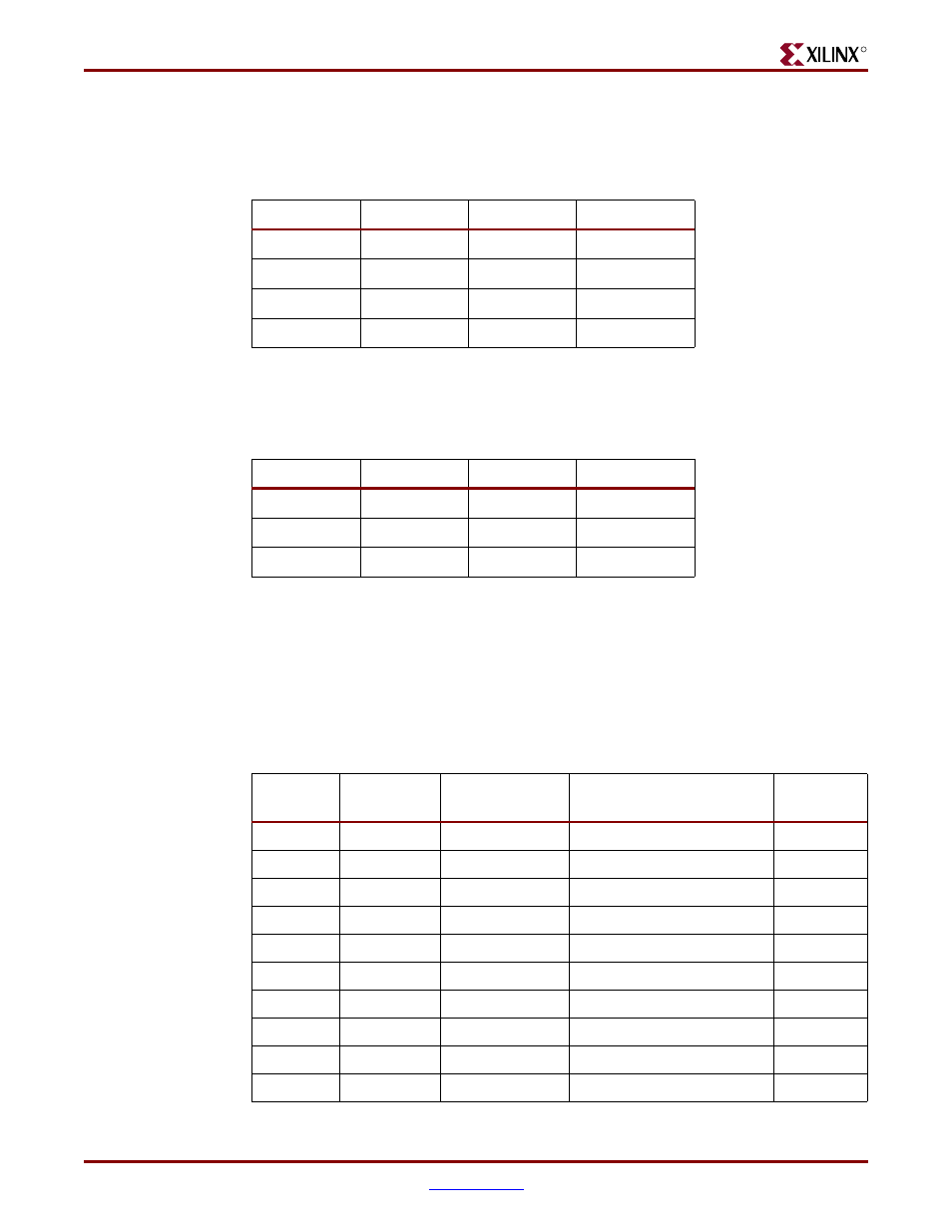
Table 2-29:
PM1 Power and Ground Pins
Pin Number
Description
Length
Contact Order
1, 6
Ground
Level 4
First
2, 5
2.5V
Level 3
Second
3
3.3V
Level 2
Third
4
1.5V
Level 2
Third
Table 2-30:
PM2 Power and Ground Pins
Pin Number
Description
Length
Contact Order
1, 6
Ground
Level 4
First
2, 5
5V
Level 3
Second
3, 4
12V
Level 2
Third
Table 2-31:
PM1 Pinout
PM1 Pin
FPGA Pin
Pin Description
ML310 Schematic Net
FPGA Bank
V
CCO
A1
H26
IO_L32P_7
PM_IO_94
2.5V
A2
H25
IO_L32N_7
PM_IO_95
2.5V
A3
D26
IO_L03P_7
PM_IO_86
2.5V
A4
C26
IO_L03N_7
PM_IO_87
2.5V
A5
E13
IO_L46N_1
PM_IO_3V_25
3V
A6
E11
IO_L43P_1
PM_IO_3V_18
3V
A7
F10
IO_L07N_1
PM_IO_3V_7
3V
A8
H12
IO_L45P_1
PM_IO_3V_22
3V
A9
C7
IO_L08N_1
PM_IO_3V_9
3V
A10
D10
IO_L37N_1
PM_IO_3V_13
3V