Ddr signaling, Ddr memory expansion, Chapter 2: ml310 embedded development platform – Xilinx ML310 User Manual
Page 22
22
ML310 User Guide
1-800-255-7778
UG068 (v1.01) August 25, 2004
Chapter 2: ML310 Embedded Development Platform
R
DDR Signaling
The FPGA DDR DIMM interface supports SSTL2 signaling. All DDR signals are controlled
impedance and are SSTL2 terminated.
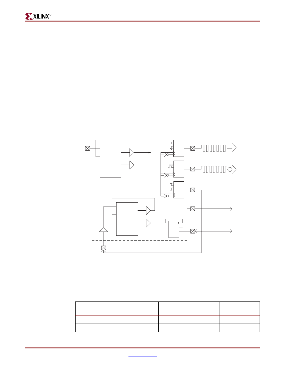
DDR Memory Expansion
The FPGA is capable of replicating up to three differential clock output pairs to the DIMM
in order to support either registered or unbuffered DIMMs. The ML310 DDR interface is
very flexible in the event different DDR memory is desired such as an unbuffered DIMM or
increased memory size. The DDR interface core delivered with EDK supports both
registered and unbuffered DRR Memory interfaces. Please review the EDK Processor IP
Reference Guide when migrating to a different DDR DIMM.
lists the connections from the FPGA to the DDR DIMM interface. Please note that
the DDR_DQ signal names do not correlate as the FPGA uses IBM notation, Big Endian,
while the DDR DIMMs use Intel notation, Little Endian.
Figure 2-4:
DDR DIMM Interface Block Diagram
Table 2-1:
Connections from FPGA to DIMM Interface, P7
UCF Signal Name
XC2VP30 Pin
(U37)
Schem Signal Name
DIMM
(P7)
ddr_ad[0]
AE23
DDR_A0
48
ddr_ad[1]
AJ23
DDR_A1
43
IBUFG
BUFG
BUFG
D0
D1
C0
C1
FDDRSE
D0
D1
C0
C1
FDDRSE
D0
D1
C0
C1
FDDRSE
CLK90
CLK0
CLKIN
CLKFB
BUFG
BUFG
CLK90
CLK0
CLKIN
CLKFB
C
CE
D
Q
DQS_i
DDR_CLK90_in
DDR DIMM (P7)
(U37)
DDR_DQ/DQS
DDR_CLK_FB_out
DDR_CLK_N
DDR_CLK
PLB_CLK
CLK90_IN
DCM
DCM
DDR_CLK_FB_in
LVCMOS
25
SSTL2_I
SSTL2_I
SSTL2_II
ADDR
DDR Control
SSTL2_I
LVCMOS
25
Phase Shift