Xilinx ML310 User Manual
Page 56
56
ML310 User Guide
1-800-255-7778
UG068 (v1.01) August 25, 2004
Chapter 2: ML310 Embedded Development Platform
R
The front panel interface provides the following status information available at the J23
header.
♦
FPGA Configuration DONE
-
Output intended for driving an LED
♦
IDE Disk access
-
Output intended for driving an LED
♦
ATX Power
-
Output intended for driving an LED
♦
2 FPGA User Defined Signals
-
Outputs intended for driving LEDs
♦
ATX Speaker
-
Output, see Ali M1535D+ data sheet for more details
♦
Keyboard Inhibit (active low input)
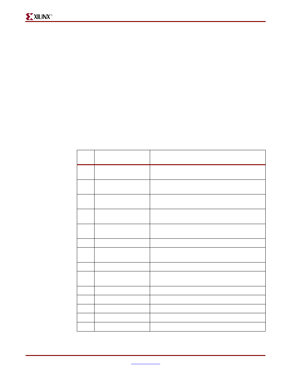
shows the signals available at the Front Panel Interface header, J23.
Table 2-25:
Front Panel Interface connector, J23
J23
Pin
Schem Signal
Description
1
SYACE_CFGA0
Used to select System ACE configuration,
CFGADDR0
2
FPGA_USER_LED1
User Defined function, Connects to XC2VP30, U37-
AH10, (2.5V Bank)
3
SYACE_CFGA1
Used to select System ACE configuration,
CFGADDR1
4
FPGA_USER_LED2
User Defined function, Connects to XC2VP30, U37-
AC14, (2.5V Bank)
5
SYACE_CFGA2
Used to select System ACE configuration,
CFGADDR2
6
NC
No Connect
7
LED_DONE_R
Remote FPGA DONE indicator, Tie this pin to Anode
of user’s LED and Cathode to GND
8
GND
Ground
9
ATX_PWRLED
ATX 3.3V power indicator, Tie this pin to Anode of
user’s LED and Cathode to GND
10
ATX_SPKR
Used to drive user defined ATX Speaker input
11
NC
No Connect
12
NC
No Connect
13
GND
Ground
14
GND
Ground