Xilinx ML310 User Manual
Page 38
38
ML310 User Guide
1-800-255-7778
UG068 (v1.01) August 25, 2004
Chapter 2: ML310 Embedded Development Platform
R
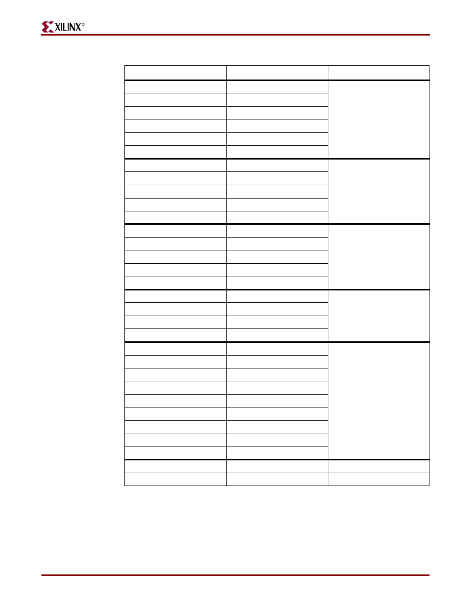
PCI_INTA
L5
PCI Interrupt Signals
PCI_INTB
N2
PCI_INTC
M2
PCI_INTD
R9
PCI_INTE
P9
PCI_INTF
M3
PCI_REQ0_N
P1
PCI Request Signals
PCI_REQ1_N
N1
PCI_REQ2_N
P7
PCI_REQ3_N
P8
PCI_REQ4_N
N3
PCI_GNT0_N
P2
PCI Grant Signals
PCI_GNT1_N
P3
PCI_GNT2_N
R7
PCI_GNT3_N
R8
PCI_GNT4_N
P4
PCI_CBE[0]
J2
PCI Byte Enable Signals
PCI_CBE[1]
H2
PCI_CBE[2]
M7
PCI_CBE[3]
M8
PCI_FRAME_N
K6
PCI Control Signals
PCI_IRDY_N
K1
PCI_TRDY_N
J1
PCI_STOP_N
M5
PCI_DEVSEL_N
M6
PCI_PERR_N
J3
PCI_SERR_N
J4
PCI_LOCK
L2
PCI_IDSEL
K2
PCI_REQ64_N*
F8
# PM_IO_3V_1
PCI_ACK64_N*
E8
# PM_IO_3V_2
Table 2-10:
PCI Controller Connections (Continued)
UCF Signal Name
XC2VP30 Pin (U37)
Description