Xilinx ML310 User Manual
Page 51
ML310 User Guide
51
UG068 (v1.01) August 25, 2004
1-800-255-7778
Board Hardware
R
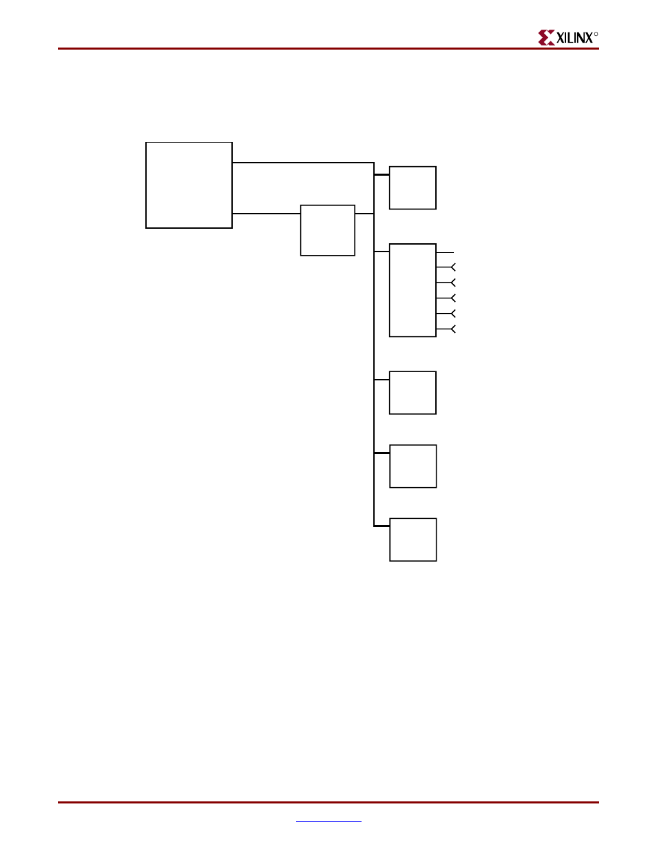
shows a block diagram of the FPGA in relation to the SMBus accelerator and the
IIC bus.
Note:
Either the XC2VP30 or the ALi M1535D+ can master the IIC bus but not simultaneously
Figure 2-14:
SMBus and IIC Block Diagram
U37
Virtex-II Pro
FPGA
XC2VP30
U15
ALi
Southbridge
M1535 D+
U27
SMBUS
Accelerator
ADDR:
0x5C
ADDR:
0xA2
RTClock
ADDR:
0xA0
EEPROM
SPD
EEPROM
Voltage
Temp
Monitor
LTC1694
Temperature
U20
LM87
VCC12V_P
VCC5V
VCC2V5
VVCC3_PCI
VCC1V5
IIC Bus
PCI Bus
U22
RTC8566
U21
24LC64
P7
Note: Located on
DDR DIMM P7